What is a Rigid-Flex PCB?
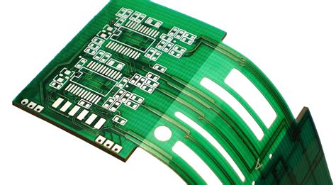
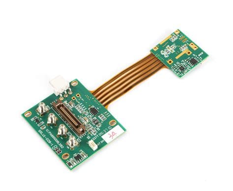
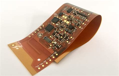
A rigid-flex PCB, also known as a rigid-flexible circuit board, combines the best of both rigid and flexible PCBs. It consists of multiple layers of flexible PCB substrates attached to one or more rigid PCB sections. The flexible parts allow the board to be bent and folded into nearly any configuration to fit the space constraints of the device it’s used in.
Rigid-flex PCBs offer several advantages over using separate rigid and flex circuits connected by wires or connectors:
- Fewer interconnections are needed, improving reliability
- The flexible substrate can be folded to fit into tight, compact, or unusual spaces
- Flex circuits can be combined with rigid PCBs for localized flexibility where needed
- Rigid sections provide mechanical support and stability for components
- Assembly is simplified since the rigid and flex portions are integrated
Rigid-Flex PCB Structure
A rigid-flex PCB typically has multiple layers consisting of:
- Flexible PCB substrates made of polyimide, PEEK, or other thin, flexible materials
- Adhesives to bond the flexible layers together
- Copper traces for conducting signals
- Coverlay or soldermask for protection
- Rigid FR-4 sections for mounting components
The flexible layers are laminated together, typically in symmetrical stack-ups to prevent warping, and then bonded to the rigid sections. Conductors on the flex layers connect to plated through-holes or vias in the rigid sections.
Advantages of Rigid-Flex PCBs
Space Savings
One of the biggest benefits of rigid-flex PCBs is their ability to save space. The flexible sections can be folded to fit into tight enclosures or conform to the shape of a device’s housing. This allows Rigid-Flex Designs to combine multiple rigid PCBs into one assembly, eliminating the need for bulky connectors and cables.
Weight Reduction
Rigid-flex circuits enable weight savings by using thinner materials than rigid PCBs. Polyimide films used in flex layers are typically 0.002″ or less in thickness. Eliminating heavy connectors also contributes to weight reduction. In aerospace and portable devices, every gram matters.
Improved Reliability
Every connector and cable is a potential point of failure. Vibration and repeated plugging/unplugging can cause issues over time. By integrating rigid and flex circuits into one PCB, many interconnects can be eliminated, improving reliability. Flex circuits also have good vibration resistance.
Better Signal Integrity
Rigid-flex boards can have controlled impedance traces for high speed signals. The polyimide material used in flex layers has stable dielectric properties. Eliminating connectors also reduces unwanted signal reflections. Rigid-flex PCBs allow shorter signal paths than designs with multiple rigid boards.
Design Flexibility
Rigid-flex technology gives designers more freedom to optimize the layout in three dimensions. Flex layers can be shaped to route conductors around obstacles. Rigid sections can be placed in different planes. Rigid-flex PCBs can thus enable new product designs not possible with rigid boards alone.

Disadvantages of Rigid-Flex PCBs
Higher Cost
The main drawback of rigid-flex PCBs is their higher cost compared to rigid-only boards. Flex materials, extra processing steps, skilled labor, and specialized equipment all add to the cost. Rigid-flex designs require extremely accurate layer registration. Most PCB shops are not capable of building rigid-flex boards, so the pool of potential suppliers is smaller.
Longer Lead Times
Fabricating rigid-flex PCBs is more complex than making rigid-only boards. Cycles of lamination, drilling, plating, and inspection are needed for the flexible and rigid portions. The multiple lamination cycles take more time. Extra care is required to get the flex-to-rigid transitions right. Expect lead times of 3-5 weeks for rigid-flex orders versus 1-2 weeks for rigid PCBs.
Design Complexity
Rigid-Flex PCB Design requires specialized knowledge beyond typical rigid board design. Critical factors include bend radius control, stiffener design, flex-to-rigid transition areas, layer stack-up, and material selection. Mechanical CAD tools, not just electronic CAD, are needed to ensure the flex circuit will fit the enclosure. Multiple design iterations and prototypes are common.

Rigid-Flex PCB Applications
Rigid-flex PCBs are used in a variety of industries and applications where space savings, reliability, and design flexibility are important. Some examples include:
Aerospace and Defense
- Avionics
- Satellites
- Missiles
- Wearable systems for soldiers
Medical Devices
- Implantable electronics
- Diagnostic equipment
- Monitoring systems
- Surgical tools
Consumer Electronics
- Smartphones
- Wearables
- Cameras
- Gaming systems
Industrial
- Robotics
- Instrumentation
- Control systems
- Portable test equipment
Automotive
- Engine control units
- Sensors
- Infotainment systems
- Driver assistance features

How to Design a Rigid-Flex PCB
Designing a rigid-flex PCB requires careful planning and attention to detail. Here are some key considerations:
Choose the Right Materials
The flexible substrate material should be able to withstand the expected number of flex cycles over the product’s lifetime. Polyimide films are a common choice. For high-reliability applications, polyimide adhesives may be used instead of acrylic. Copper weights of 0.5 oz to 1 oz are typical for flex layers.
Determine the Layer Stack-up
Rigid-flex PCBs can have complex layer stack-ups with multiple flex and rigid sections. The stack-up design affects signal integrity, impedance control, EMI, and manufacturability. In general, use balanced stack-ups that are symmetrical around the center layer to prevent warping. Use enough layers to route all signals without crossing flex-to-rigid boundaries more than necessary.
Minimize Bend Radius
The minimum bend radius depends on the thickness and materials of the flex layers. In general, thicker layers require larger bend radii. The bend radius should be at least 6 times the total thickness of the flex section. Tighter bends put more stress on the copper traces and can cause cracks over time.
Avoid Traces in Bend Areas
Copper traces should not be routed through the bend areas of the flex circuit whenever possible. If unavoidable, use curved traces perpendicular to the bend direction. Hatched polygons can provide flexibility in bend areas. Traces in bends are more likely to crack under repeated flexing.
Manage Flex-to-Rigid Transitions
The transition areas where the flex layers meet the rigid sections require special attention. Copper pads should be teardrop-shaped, not round, to prevent stress concentrations. Traces should enter pads at angles, not straight in. Vias should be filled and planar to prevent flex layers from tearing. Use hatched polygons to distribute stress. Stiffeners can be added to control the flexing areas.
Allow for Layer Registration Tolerance
The flexible layers must be aligned very precisely with each other and with the rigid sections. However, some registration tolerance is inevitable. Traces and vias should be designed with allowance for layer misalignment, typically 0.005″ or more. Larger vias, min trace width, and clearances are needed compared to rigid PCBs.
Consider Panelization and Routing
Rigid-flex PCBs are often panelized to fit multiple boards on one panel for efficiency. The flex areas should be oriented to minimize waste and allow the panel to lie flat. V-score or tab routing can be used to separate individual boards. The flex areas may need to be stiffened during assembly to allow SMT placement.
Rigid-Flex PCB Manufacturing Process
The manufacturing process for rigid-flex PCBs is more complex than for rigid boards alone. Here is an overview of the basic steps:
- Create the flexible layers
- Print and etch the circuits on thin copper-clad laminates
- Cut out the flex substrates to size using steel-rule dies or lasers
- Laminate the flex layers with coverlay using heat and pressure
- Fabricate the rigid layers
- Print and etch the circuits on rigid PCB substrates
- Drill holes for component mounting and vias
- Deposit copper in the holes to create plated through-holes
- Laminate the rigid and flexible sections together
- Lay up the flex and rigid substrates with adhesives
- Apply heat and pressure to bond the layers
- Drill holes in the rigid sections
- Plate the holes with copper to connect the layers
- Route out the individual boards
- Remove excess material using routing or punching
- Add soldermask and silkscreen
- Test and inspect the finished boards
Rigid-flex PCB manufacturing requires specialized equipment and expertise. The lamination process is critical to ensure good adhesion between the layers. The flex-to-rigid transition areas must be carefully designed and fabricated to prevent delamination or cracking. Registration of the layers must be tightly controlled. Few PCB shops have the capability to build rigid-flex boards.
Selecting a Rigid-Flex PCB Supplier
When choosing a supplier for rigid-flex PCBs, consider the following:
- Technical Capabilities: Can they fabricate boards with the layer count, materials, features, and tolerances your design requires?
- Experience: How long have they been building rigid-flex PCBs? What industries and applications do they serve?
- Quality: What certifications, inspection methods, and test procedures do they use to ensure quality?
- Support: Can they provide design reviews, DFM feedback, and technical advice to help optimize your design?
- Capacity: How many boards can they produce per week or month? What are their typical lead times?
- Cost: Are their prices competitive? Do they offer discounts for volume orders?
It’s a good idea to get quotes from multiple rigid-flex PCB suppliers and compare their capabilities, pricing, and lead times. Look for a supplier that has experience with your type of application and can meet your technical and quality requirements.
Rigid-Flex PCB Design Tools
To design rigid-flex PCBs, you’ll need CAD tools that support flex circuit design. Here are some popular options:
| Tool | Vendor | Features |
|---|---|---|
| PADS Professional | Mentor Graphics | 3D Multi-Board Design, flex/rigid-flex support, simulation |
| Altium Designer | Altium | Layer stack manager, rigid-flex rules, 3D modeling |
| OrCAD/Allegro | Cadence | Rigid-flex design rules, constraint manager, MCAD co-design |
| EAGLE | Autodesk | Schematic capture, PCB layout, flex support (requires add-on) |
| Xpedition Enterprise | Mentor | Rigid-flex layout, stack-up editor, multi-board design |
Most of these tools offer schematic capture, PCB layout, routing, and 3D modeling capabilities. They also have specific features for rigid-flex design, such as layer stack management, bend radius control, and design rule checks. Some tools can import mechanical CAD models to ensure the PCB fits the enclosure. Others can export 3D models of the PCB for mechanical interference checking.
Whichever tool you choose, make sure it has the capabilities needed for your specific rigid-flex design. Work with your manufacturer to ensure the design meets their fabrication requirements. Get training on the tool’s flex-specific features to avoid common design mistakes.
FAQ
What is the cost difference between rigid and rigid-flex PCBs?
Rigid-flex PCBs are typically 2-5 times more expensive than comparable rigid PCBs. The higher cost is due to the specialized materials, equipment, and labor required. Flex substrates and adhesives cost more than FR-4. Extra processing steps are needed to laminate the flex layers and bond them to the rigid sections. Yield is often lower due to the tight tolerances and registration required.
How long do rigid-flex PCBs last?
The lifespan of a rigid-flex PCB depends on factors such as the materials, number of flex cycles, bend radius, and environmental conditions. With proper design and fabrication, rigid-flex boards can last for tens of thousands of flex cycles. The flexible substrates are rated for millions of cycles, but the copper traces are more likely to fail due to fatigue.
In general, rigid-flex PCBs are very reliable and can last for many years in applications with infrequent flexing. For high-cycle applications, such as printer mechanisms or medical catheters, the design must be carefully optimized for the expected flex life. Using thinner layers, larger bend radii, and stress relief features can help extend the lifespan.
What industries commonly use rigid-flex PCBs?
Rigid-flex PCBs are used in a variety of industries where size, weight, and reliability are critical. Some of the most common applications include:
- Aerospace and defense: avionics, satellites, missiles, wearable systems
- Medical devices: implantable electronics, surgical tools, monitoring equipment
- Consumer electronics: smartphones, wearables, gaming systems, VR/AR headsets
- Industrial automation: robotics, sensors, control systems, test equipment
- Automotive: engine control units, infotainment systems, driver assistance features
Rigid-flex PCBs are also used in applications where the device must conform to the shape of the human body, such as hearing aids, fitness trackers, and medical implants. The ability to fold the flex layers allows the PCB to fit into ergonomic enclosures.
What are the most common materials used in rigid-flex PCBs?
The most common materials used in rigid-flex PCBs are:
- Flexible substrates: polyimide films (Kapton), polyester films (Mylar), PEEK films
- Adhesives: acrylic, epoxy, or polyimide-based adhesives
- Copper: electrodeposited or rolled annealed copper in weights of 0.5 oz to 1 oz per square foot
- Soldermask: flexible photoimageable soldermask or coverlay films
- Stiffeners: FR-4, polyimide, or aluminum layers to control bend areas
- Rigid substrates: FR-4, high-Tg FR-4, or polyimide-glass laminates
The choice of materials depends on the specific application requirements, such as temperature range, chemical resistance, dielectric properties, and flexibility. Polyimide films are the most common choice for flex layers due to their high strength, heat resistance, and stability. Adhesiveless substrates, such as liquid crystal polymer (LCP), are used in high-frequency applications.
How do you specify a rigid-flex PCB Stackup?
Specifying a rigid-flex PCB stackup involves defining the number, type, and order of the layers, as well as the materials and thicknesses of each layer. Here are some key considerations:
- Number of layers: Determine how many copper layers are needed for routing, power, and ground planes. More layers increase cost and complexity.
- Flexible layers: Decide how many flex layers are needed and where they will be located in the stackup. Flex layers are typically placed in pairs to create a symmetrical stackup that balances stresses.
- Rigid layers: Determine how many rigid layers are needed and where they will be located. Rigid layers provide mechanical support and allow through-hole components.
- Materials: Specify the type and thickness of the flexible substrate, adhesives, copper, soldermask, and rigid substrate materials.
- Copper weights: Choose the copper weights for each layer based on the current carrying and trace width requirements. Thinner copper is more flexible but has higher resistance.
- Adhesives: Select the type and thickness of adhesives to bond the layers together. Thicker adhesives provide better isolation but reduce flexibility.
- Overall thickness: Calculate the total thickness of the stackup based on the layer thicknesses and adhesives. Thicker stackups are less flexible and more expensive.
Here is an example stackup for a 6-layer rigid-flex PCB:
| Layer | Material | Thickness (mm) |
|---|---|---|
| Top cover | Polyimide film | 0.025 |
| Top flex | Copper (0.5 oz) | 0.018 |
| Flex core | Polyimide film | 0.050 |
| Bottom flex | Copper (0.5 oz) | 0.018 |
| Adhesive | Acrylic | 0.050 |
| Top rigid | FR-4 | 0.200 |
| Inner rigid 1 | Copper (1 oz) | 0.035 |
| Inner rigid 2 | Copper (1 oz) | 0.035 |
| Bottom rigid | FR-4 | 0.200 |
The stackup shows a symmetrical arrangement of flex layers in the center, bonded to rigid layers on the top and bottom. The overall thickness is 0.631 mm (24.8 mils). The rigid layers provide mechanical support and allow through-hole components, while the flex layers allow the board to bend in the middle.
Work with your rigid-flex PCB supplier to optimize the stackup for your specific design requirements. They can provide guidance on material selection, layer arrangement, and manufacturability. Be sure to consider the bend radius, flex life, and signal integrity requirements when specifying the stackup.
Conclusion
Rigid

No responses yet