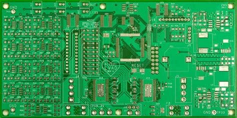
Introduction to PCB stackup
In the world of electronic design, Printed Circuit Boards (PCBs) play a crucial role in connecting and supporting various components to create a functional device. As devices become more complex and compact, designers often turn to multi-layer PCBs to accommodate the increasing number of components and intricate connections. This is where the concept of PCB stackup comes into play.
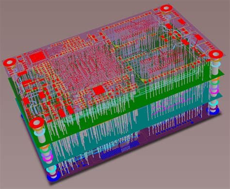
PCB stackup refers to the arrangement of copper layers and insulating materials that make up a multi-layer PCB. It is a critical aspect of PCB design, as it determines the overall thickness, signal integrity, and manufacturing feasibility of the board. A well-designed PCB stackup ensures proper signal routing, minimizes crosstalk and electromagnetic interference (EMI), and facilitates efficient manufacturing processes.
The Importance of PCB stackup design
Signal Integrity
One of the primary reasons for implementing a multi-layer PCB stackup is to maintain signal integrity. As the number of components and connections increases, the risk of signal degradation, crosstalk, and EMI also rises. By strategically arranging the copper layers and using appropriate insulating materials, designers can minimize these issues and ensure reliable signal transmission throughout the board.
Board Thickness and Density
PCB stackup design also plays a significant role in determining the overall thickness and component density of the board. With the growing demand for smaller and more compact devices, designers must find ways to accommodate a large number of components within a limited space. Multi-layer PCBs allow for higher component density by utilizing the vertical space, enabling designers to create thinner and more compact boards.
Manufacturing Feasibility
A well-designed PCB stackup not only ensures optimal performance but also facilitates efficient manufacturing processes. The choice of materials, layer arrangement, and via placement can impact the manufacturability of the board. By considering manufacturing constraints and best practices during the stackup design phase, designers can avoid potential issues and ensure a smooth production process.
Factors to Consider in PCB Stackup Design
Number of Layers
The number of layers in a PCB stackup depends on the complexity of the device and the routing requirements. A simple device may only require a two-layer board, while more complex devices may need four, six, or even more layers. Determining the appropriate number of layers involves careful consideration of signal routing, power distribution, and component placement.
Material Selection
The choice of materials for the PCB stackup is crucial for ensuring the desired electrical properties and reliability. The most common materials used in PCB fabrication are FR-4, a glass-reinforced epoxy laminate, and copper foil for the conductive layers. Other materials, such as high-frequency laminates or flexible substrates, may be used for specific applications or to meet certain performance requirements.
Layer Arrangement
The arrangement of copper layers in a PCB stackup plays a significant role in signal integrity and EMI reduction. A typical four-layer stackup consists of a top signal layer, a ground plane, a power plane, and a bottom signal layer. This arrangement provides a low-impedance path for power distribution and helps to minimize crosstalk between signal layers. In more complex designs, additional signal layers and ground planes may be added to improve signal routing and shielding.
Via Placement and Design
Vias are conductive pathways that connect different layers of a PCB. The placement and design of vias in a PCB stackup can impact signal integrity and manufacturing feasibility. Designers must consider via size, spacing, and proximity to other components to ensure proper signal transmission and avoid manufacturing issues such as drill breakout or via-in-pad problems.

Common PCB Stackup Configurations
Four-Layer Stackup
A four-layer PCB stackup is a common configuration for moderately complex devices. It consists of the following layers:
1. Top Signal Layer
2. Ground Plane
3. Power Plane
4. Bottom Signal Layer
This arrangement provides a good balance between signal routing, power distribution, and EMI reduction. The ground and power planes act as reference planes for the signal layers, helping to maintain signal integrity and minimize crosstalk.
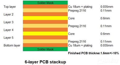
Six-Layer Stackup
For more complex devices with higher component density and routing requirements, a six-layer PCB stackup may be necessary. A typical six-layer stackup consists of:
1. Top Signal Layer
2. Ground Plane
3. Inner Signal Layer 1
4. Power Plane
5. Inner Signal Layer 2
6. Bottom Signal Layer
The additional signal layers in a six-layer stackup provide more routing options and help to reduce the overall board size. The ground and power planes serve the same purpose as in a four-layer stackup, providing reference planes and reducing EMI.
High-Density Interconnect (HDI) Stackup
HDI PCBs are designed to accommodate extremely high component density and complex routing requirements. These boards often feature micro-vias, buried vias, and blind vias to maximize routing density. A typical HDI stackup may consist of eight or more layers, with multiple signal layers and ground planes.
HDI stackups require careful design considerations to ensure signal integrity and manufacturability. The use of advanced materials, such as low-loss laminates and high-density copper foils, is often necessary to meet the stringent performance requirements of HDI designs.
PCB Stackup Design Considerations
Signal Routing
Proper signal routing is essential for maintaining signal integrity and minimizing crosstalk in a PCB stackup. Designers should follow best practices, such as keeping signal traces as short as possible, avoiding sharp bends, and maintaining consistent trace widths. Differential pairs should be routed closely together to maintain signal balance and reduce EMI.
Power Distribution
Efficient power distribution is crucial for ensuring the stable operation of components in a PCB stackup. The power plane should be designed to provide a low-impedance path for current flow, minimizing voltage drops and ensuring consistent power delivery to all components. Decoupling capacitors should be placed close to power-hungry components to suppress high-frequency noise and maintain Power Integrity.
Grounding and Shielding
Proper grounding and shielding techniques are essential for reducing EMI and maintaining signal integrity in a PCB stackup. The ground plane should provide a low-impedance return path for signals and help to shield sensitive components from external noise sources. Stitching vias can be used to connect ground planes on different layers, creating a continuous shield that reduces EMI.
Thermal Management
As component density increases in a PCB stackup, thermal management becomes a critical consideration. Designers must ensure that heat generated by components can be efficiently dissipated to prevent performance degradation and reliability issues. Thermal vias can be used to transfer heat from components to the ground plane or dedicated thermal layers, helping to spread the heat and improve overall thermal performance.
Manufacturing Considerations
Designing a PCB stackup that is easy to manufacture is essential for reducing costs and ensuring a reliable end product. Designers should consider the capabilities and limitations of the PCB fabrication process, such as minimum trace widths, via sizes, and drill capabilities. It is also important to adhere to industry standards and guidelines, such as the IPC-2221 standard for PCB design, to ensure compatibility with established manufacturing processes.
PCB Stackup Materials
FR-4
FR-4 is the most commonly used material for PCB fabrication. It is a glass-reinforced epoxy laminate that offers good mechanical strength, thermal stability, and electrical insulation properties. FR-4 is suitable for a wide range of applications and is relatively inexpensive compared to other PCB materials.
High-Frequency Laminates
For applications that require high-speed signal transmission or operate at high frequencies, specialized laminates may be necessary. These materials, such as Rogers RO4000 series or Isola IS410, offer lower dielectric constants and dissipation factors, which help to reduce signal loss and maintain signal integrity at high frequencies. High-frequency laminates are more expensive than FR-4 and may require specialized manufacturing processes.
Flexible Substrates
Flexible PCBs are increasingly used in applications that require conformity to non-planar surfaces or where space is limited. These boards are made using flexible substrates, such as polyimide or polyester, which allow the PCB to bend and flex without damaging the circuits. Flexible PCBs require special design considerations, such as the use of stretchable conductors and the placement of components to minimize stress during flexing.
Copper Foil
Copper foil is used for the conductive layers in a PCB stackup. The thickness of the copper foil is typically measured in ounces per square foot (oz/ft²), with common thicknesses ranging from 0.5 oz/ft² to 2 oz/ft². Thicker copper foils offer lower resistance and higher current-carrying capacity but may be more challenging to etch and route. Thinner copper foils are easier to work with but may have higher resistance and lower current-carrying capacity.
PCB Stackup Design Tools
CAD Software
Computer-Aided Design (CAD) software is an essential tool for creating and managing PCB stackup designs. Popular CAD tools for PCB design include Altium Designer, Cadence Allegro, and Mentor Graphics PADS. These tools offer features such as schematic capture, 3D modeling, and automated design rule checking (DRC) to help designers create accurate and manufacturable PCB stackups.
Simulation Tools
Simulation tools are used to analyze the performance of a PCB stackup before fabrication. These tools can help designers optimize signal integrity, power distribution, and thermal performance by simulating the behavior of the board under various operating conditions. Popular simulation tools include Ansys SIwave, Mentor Graphics HyperLynx, and Cadence Sigrity.
Collaboration Platforms
Collaboration platforms enable designers to share and review PCB stackup designs with team members, suppliers, and manufacturers. These platforms facilitate communication and help to streamline the design process by providing a centralized repository for design files, feedback, and revisions. Examples of collaboration platforms for PCB design include Altium 365, Cadence OrbitIO, and Upverter.
PCB Stackup Best Practices
Follow Industry Standards
Adhering to industry standards, such as IPC-2221 for PCB design and IPC-4101 for PCB materials, ensures that your PCB stackup design is compatible with established manufacturing processes and meets the required quality and reliability standards. Following these standards also helps to minimize the risk of design errors and manufacturing issues.
Keep It Simple
While it may be tempting to create a complex PCB stackup with numerous layers and intricate routing, it is often best to keep the design as simple as possible. A simpler design is easier to manufacture, less prone to errors, and more cost-effective. Only add layers and complexity when necessary to meet the specific requirements of your application.
Collaborate with Manufacturers
Engaging with PCB manufacturers early in the design process can help to ensure that your PCB stackup is optimized for manufacturability. Manufacturers can provide valuable insights into material selection, layer arrangement, and design rules that can help to minimize manufacturing issues and reduce costs. Establishing a strong collaboration with your manufacturing partners can lead to a more efficient and reliable end product.
Test and Validate
Before finalizing your PCB stackup design, it is essential to test and validate its performance through simulations and prototypes. Simulations can help to identify potential signal integrity, power distribution, and thermal issues, allowing you to make necessary adjustments before committing to fabrication. Building and testing prototypes can further validate the design and ensure that it meets the desired performance and reliability requirements.
Document and Communicate
Clear documentation and communication are critical for the success of a PCB stackup design project. Ensure that all design files, specifications, and requirements are properly documented and shared with all stakeholders, including team members, suppliers, and manufacturers. Effective communication helps to avoid misunderstandings, reduces the risk of errors, and facilitates a smooth design and manufacturing process.
Frequently Asked Questions (FAQ)
1. What is the difference between a four-layer and six-layer PCB stackup?
A four-layer PCB stackup consists of two signal layers, a ground plane, and a power plane, while a six-layer stackup adds two additional signal layers. The extra layers in a six-layer stackup provide more routing options and help to reduce the overall board size, making it suitable for more complex devices with higher component density and routing requirements.
2. How does the choice of materials affect PCB stackup performance?
The choice of materials in a PCB stackup can significantly impact its electrical properties, thermal performance, and mechanical stability. For example, using high-frequency laminates with lower dielectric constants and dissipation factors can help to reduce signal loss and maintain signal integrity at high frequencies. Flexible substrates, such as polyimide, allow for the creation of flexible PCBs that can conform to non-planar surfaces.
3. What is the role of vias in a PCB stackup?
Vias are conductive pathways that connect different layers of a PCB stackup. They allow signals to travel between layers, enabling more complex routing and higher component density. The placement and design of vias can impact signal integrity and manufacturing feasibility, so designers must carefully consider via size, spacing, and proximity to other components.
4. How can I ensure my PCB stackup is manufacturable?
To ensure your PCB stackup is manufacturable, consider the capabilities and limitations of the PCB fabrication process, such as minimum trace widths, via sizes, and drill capabilities. Adhere to industry standards and guidelines, such as the IPC-2221 standard for PCB design, and collaborate with manufacturers early in the design process to optimize your stackup for manufacturability.
5. What tools are available for designing and simulating PCB stackups?
Several tools are available for designing and simulating PCB stackups. CAD software, such as Altium Designer, Cadence Allegro, and Mentor Graphics PADS, offers features for creating and managing PCB stackup designs. Simulation tools, like Ansys SIwave, Mentor Graphics HyperLynx, and Cadence Sigrity, help designers analyze the performance of a PCB stackup before fabrication, optimizing signal integrity, power distribution, and thermal performance.
Conclusion
PCB stackup design is a critical aspect of creating complex, multi-layer PCBs for advanced electronic devices. By carefully considering factors such as the number of layers, material selection, layer arrangement, and via placement, designers can create PCB stackups that offer optimal signal integrity, power distribution, and thermal performance while ensuring manufacturability and reliability.
Adhering to best practices, such as following industry standards, keeping designs simple, collaborating with manufacturers, testing and validating, and maintaining clear documentation and communication, can help streamline the PCB stackup design process and lead to a successful end product.
As electronic devices continue to become more complex and compact, the importance of effective PCB stackup design will only continue to grow. By staying up-to-date with the latest design techniques, materials, and tools, PCB designers can create multi-layer circuits that meet the ever-increasing demands of modern electronic applications.
No responses yet