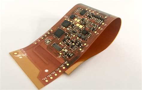
Introduction to Rigid-flex PCBs
A rigid-flex PCB combines rigid and flexible substrates laminated together into a single circuit. The rigid parts of the board contain traditional FR4 PCB material and components. The flexible portions use thin, bendable plastic substrates that allow the board to flex and even fold. This enables 3D configurations, reduced space and weight, and dynamic flexing.
Rigid-flex PCBs offer many advantages over traditional rigid boards:
- Reduced size and weight by replacing multiple rigid PCBs and connectors
- Improved reliability by eliminating connectors and solder joints
- 3D design capability for installing boards in tight spaces
- Dynamic flexing for movable mechanisms like hinges
- Better signal integrity and EMC due to shorter traces
Key Design Considerations for Rigid-flex PCBs
Board stack-up and materials
The stack-up of a rigid-flex PCB consists of alternating rigid and flexible layers laminated together. The rigid layers use standard FR4 material and copper weights. The flexible layers use thin polyimide substrates with copper on one or both sides.
Here is an example 6-layer rigid-flex stack-up:
| Layer | Material | Thickness |
|---|---|---|
| Top overlay | ||
| Top copper | 1 oz Cu | 0.0014″ |
| Prepreg | FR4 | 0.0040″ |
| L2 copper | 0.5 oz Cu | 0.0007″ |
| Core | FR4 | 0.0079″ |
| L3 copper | 1 oz Cu | 0.0014″ |
| Prepreg | FR4 | 0.0040″ |
| L4 copper | 0.5 oz Cu | 0.0007″ |
| Coverlay | Polyimide | 0.0020″ |
| L5 copper | 0.5 oz Cu | 0.0007″ |
| Polyimide | 0.0020″ | |
| L6 copper | 0.5 oz Cu | 0.0007″ |
| Bottom overlay |
The stack-up uses 1 oz and 0.5 oz copper on the rigid layers and 0.5 oz copper on the flex layers. FR4 core and prepreg bond the rigid layers while polyimide film insulates the flex layers.
Flexible circuit routing
Routing the flexible circuit portions requires following some key guidelines to ensure reliability:
- Avoid 90° trace corners, use curved traces instead
- Maintain uniform trace width and spacing in flex regions
- Stagger traces to avoid I-beams that concentrate bending stress
- Use hatched copper planes instead of solid floods
- Limit copper plating to 1 oz max on flex layers
- Provide strain relief at rigid-flex boundaries
Following these rules minimizes mechanical stress on the traces during flexing to prevent fatigue failures.
Component placement
Component placement on rigid-flex boards focuses on keeping parts on the rigid portions as much as possible. Follow these guidelines:
- Locate all components on rigid layers, avoid placing parts on flex
- Allow adequate space around flex circuit regions for bending
- Provide additional stiffeners and support for heavy components
- Orientate components to minimize board thickness in flex areas
- Consider the assembly process and how the board will be folded
Careful component placement ensures the board is manufacturable, reliable, and can flex as needed.
3D modeling
Creating a 3D model is crucial for rigid-flex designs to ensure proper fit and clearances. Use ECAD and MCAD co-design tools to:
- Define the rigid-flex stack-up and board outline
- Determine component placement and clearances
- Identify potential collision and interference issues
- Optimize the flexible circuit bends and folds
- Analyze mechanical stresses and strains during flexing
A detailed 3D model verifies the rigid-flex board can be assembled and operate as intended in the final product enclosure.

Rigid-flex PCB Manufacturing Process
Manufacturing rigid-flex PCBs requires specialized processes and careful process control. The key steps are:
- Imaging and etching the copper traces on the rigid and flex layers
- Laminating the rigid and flex substrates together under heat and pressure
- Drilling holes and vias through the rigid and flex areas
- Plating the holes to connect traces on different layers
- Applying solder mask and silkscreen to the rigid portions
- Cutting the flex circuit regions out from the rigid panel
- Performing electrical test and inspection
The lamination and cutting steps are the most critical. Precise alignment and careful process control is needed to bond the rigid and flex layers together without damaging the thin flex materials. Special laser cutting is often used to route out the flex areas.

Design for Manufacturing Guidelines
To ensure your rigid-flex PCB is manufacturable, follow these key DFM guidelines:
- Use standard rigid and flex materials that are compatible for lamination
- Avoid using adhesiveless base materials which are more difficult to process
- Allow for panel edge clearance and rail areas that will be routed off
- Provide sacrificial material in flex areas for handling during assembly
- Call out any areas requiring special routing, drilling, or plating
- Specify all cover lay openings, stiffener requirements, and assembly instructions
- Leave ample space around flex circuit regions for the cutting process
Work closely with your fabricator and communicate your requirements clearly. Involve them early in the design process to identify any potential manufacturability issues.

FAQ
What are the advantages of rigid-flex PCBs?
Rigid-flex PCBs offer reduced size and weight, improved reliability, 3D design capability, dynamic flexing, and better signal integrity compared to rigid PCBs and connectors.
How are rigid-flex PCBs manufactured?
Rigid-flex PCBs are built by laminating alternating rigid and flexible substrates together. The main fabrication steps are imaging, lamination, drilling, plating, and cutting out the flex regions.
What special design considerations are there for flex circuits?
The key considerations are using curved traces, maintaining uniform geometry, avoiding I-beams, using hatched polygons, limiting copper thickness, and providing strain relief.
How do you optimize component placement on rigid-flex PCBs?
Place components on the rigid layers and avoid the flex regions. Allow space for flexing, provide stiffeners for heavy parts, and consider the assembly process and final folded shape.
Why is 3D modeling important for rigid-flex design?
3D modeling is critical to ensure proper fit, clearances, and flexibility in the final assembled product. It allows identifying issues and optimizing the design prior to manufacturing.
Conclusion
Rigid-flex PCBs provide a powerful option for designing circuits in products requiring reduced size, weight and dynamic flexing. However, rigid-flex design involves careful stack-up planning, flex circuit routing, component placement, and 3D modeling.
By understanding the key design requirements and manufacturing processes, you’ll be able to design rigid-flex PCBs that are reliable, manufacturable, and optimized for their intended application. Work closely with your fabricator and communicate your requirements clearly. With the right design approach, rigid-flex technology enables exciting new possibilities for electronic packaging.
No responses yet