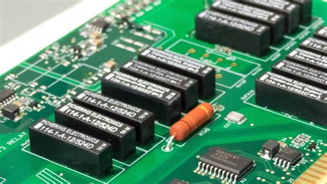
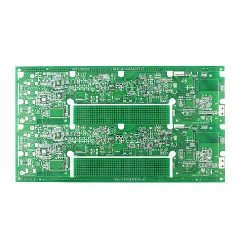
What is a PTH PCB?
A Plated Through Hole (PTH) PCB is a type of printed circuit board that features holes that are electroplated with a conductive material, typically copper, to create electrical connections between the different layers of the board. This process allows for the creation of reliable and robust electrical connections, making PTH PCBs a popular choice for a wide range of electronic applications.
The Anatomy of a PTH PCB
A typical PTH PCB consists of several layers of copper-clad laminate material, such as FR-4, which is a glass-reinforced epoxy resin. These layers are bonded together using heat and pressure, creating a solid and durable board. The copper layers are etched to create the desired circuit pattern, while the through holes are drilled and plated with copper to establish electrical connections between the layers.
The main components of a PTH PCB include:
- Substrate material (e.g., FR-4)
- Copper layers
- Solder mask
- Silkscreen
- Plated through holes
The PTH PCB Manufacturing Process
The manufacturing process for PTH PCBs involves several steps, each of which is critical to ensuring the quality and reliability of the final product.
Step 1: PCB Design
The first step in the PTH PCB manufacturing process is the design phase. This involves creating a detailed layout of the circuit using specialized PCB design software, such as Altium Designer or Eagle. The design must take into account factors such as component placement, trace width, and spacing, as well as the location and size of the through holes.
Step 2: PCB Fabrication
Once the design is complete, the next step is to fabricate the PCB. This involves the following sub-steps:
-
Copper Clad Laminate Preparation: The substrate material is cut to the desired size and shape, and the copper layers are cleaned and prepared for etching.
-
Drilling: The through holes are drilled using a computer-controlled drill machine, ensuring precise placement and size.
-
Electroplating: The drilled holes are then electroplated with copper, creating a conductive layer that connects the different layers of the board.
-
Etching: The copper layers are etched using a chemical process to remove the unwanted copper, leaving behind the desired circuit pattern.
-
Solder Mask Application: A solder mask is applied to the board to protect the copper traces and prevent accidental short circuits.
-
Silkscreen Printing: The silkscreen layer is printed onto the board, providing labels and markings for components and other important information.
Step 3: Component Assembly
After the PCB is fabricated, the next step is to assemble the components onto the board. This can be done using various methods, such as through-hole mounting or surface mount technology (SMT). Through-hole components are inserted into the plated holes and soldered in place, while SMT components are placed on the surface of the board and soldered using a reflow oven.
Step 4: Testing and Inspection
The final step in the PTH PCB manufacturing process is testing and inspection. This involves using specialized equipment to ensure that the board meets the required specifications and functions as intended. Common tests include:
- Continuity testing
- Insulation resistance testing
- Functional testing
- Visual inspection

Advantages of PTH PCBs
PTH PCBs offer several advantages over other types of PCBs, making them a popular choice for a wide range of applications.
Robust Electrical Connections
One of the main advantages of PTH PCBs is the robustness of the electrical connections. The plated through holes provide a strong and reliable connection between the different layers of the board, ensuring that the circuit functions as intended even under harsh environmental conditions.
Ease of Assembly
PTH PCBs are also relatively easy to assemble, particularly when using through-hole components. The plated holes provide a clear and convenient location for inserting and soldering the components, reducing the risk of errors and improving the overall efficiency of the assembly process.
Compatibility with Through-Hole Components
PTH PCBs are compatible with through-hole components, which are still widely used in many electronic applications. This compatibility allows for greater flexibility in component selection and can help to reduce costs in some cases.
Improved Mechanical Strength
The plated through holes in PTH PCBs also provide additional mechanical strength to the board, helping to prevent damage from vibration, shock, and other physical stresses. This can be particularly important in applications where the PCB is subjected to harsh environmental conditions or frequent handling.

Disadvantages of PTH PCBs
Despite their many advantages, PTH PCBs also have some limitations and drawbacks that should be considered when selecting a PCB technology.
Larger Footprint
PTH PCBs typically require a larger footprint than other types of PCBs, such as surface mount technology (SMT) boards. This is because the through holes take up additional space on the board, limiting the available area for components and traces.
Higher Manufacturing Costs
The manufacturing process for PTH PCBs is generally more complex and time-consuming than for other types of PCBs, which can result in higher manufacturing costs. This is particularly true for high-volume production runs or boards with a large number of through holes.
Limited Miniaturization Potential
The larger footprint and through-hole requirements of PTH PCBs can limit their potential for miniaturization. As electronic devices continue to shrink in size, this can be a significant drawback for applications that require very small or compact PCBs.

PTH PCB Applications
PTH PCBs are used in a wide range of electronic applications, from consumer electronics to industrial control systems. Some common applications include:
- Power electronics
- Automotive electronics
- Telecommunications equipment
- Medical devices
- Aerospace and defense systems
The choice of PCB technology for a particular application depends on several factors, including the required performance, environmental conditions, size constraints, and cost considerations. In many cases, PTH PCBs offer a reliable and cost-effective solution, particularly for applications that require robust electrical connections and compatibility with through-hole components.
The Future of PTH PCBs
As electronic devices continue to evolve and new technologies emerge, the role of PTH PCBs in the electronics industry is also likely to change. While the demand for PTH PCBs may decline in some areas as more manufacturers adopt surface mount technology and other advanced PCB Technologies, they are likely to remain an important option for many applications.
One potential area of growth for PTH PCBs is in the field of high-power electronics, where the robust electrical connections and mechanical strength provided by the plated through holes can be particularly valuable. Additionally, advances in materials science and manufacturing processes may help to address some of the limitations of PTH PCBs, such as their larger footprint and higher manufacturing costs.
Ultimately, the future of PTH PCBs will depend on a variety of factors, including technological advances, market demand, and the changing needs of the electronics industry. However, given their proven track record and unique advantages, it is likely that PTH PCBs will continue to play an important role in the development of electronic devices for many years to come.
FAQ
1. What is the difference between a PTH PCB and a surface mount PCB?
A PTH PCB uses plated through holes to create electrical connections between the layers of the board, while a surface mount PCB relies on surface-mounted components that are soldered directly onto the surface of the board. PTH PCBs are typically larger and more robust, while surface mount PCBs offer greater potential for miniaturization and higher component density.
2. Can PTH PCBs be used with surface mount components?
Yes, PTH PCBs can be designed to accommodate both through-hole and surface mount components. This hybrid approach can offer the best of both worlds, combining the robustness and compatibility of PTH technology with the space-saving advantages of surface mount components.
3. What materials are used in the manufacture of PTH PCBs?
The most common substrate material used in PTH PCBs is FR-4, which is a glass-reinforced epoxy resin. The conductive layers are typically made of copper, while the solder mask and silkscreen layers are made of specialized polymers designed to protect the board and provide clear labeling.
4. How are the through holes in a PTH PCB created?
The through holes in a PTH PCB are created using a computer-controlled drill machine. The holes are drilled precisely to ensure that they align with the circuit pattern on the different layers of the board. After drilling, the holes are electroplated with copper to create a conductive connection between the layers.
5. What are some of the key advantages of using PTH PCBs?
Some of the key advantages of using PTH PCBs include their robust electrical connections, ease of assembly, compatibility with through-hole components, and improved mechanical strength. These advantages make PTH PCBs a popular choice for a wide range of electronic applications, particularly those that require reliable performance in harsh environmental conditions or frequent handling.
Conclusion
PTH PCBs are a proven and reliable technology that offers several unique advantages over other types of PCBs. Their robust electrical connections, ease of assembly, and compatibility with through-hole components make them a popular choice for a wide range of electronic applications, from consumer electronics to industrial control systems.
While the larger footprint and higher manufacturing costs of PTH PCBs may limit their potential for miniaturization and high-volume production, their unique advantages continue to make them an important option for many applications. As new technologies emerge and the needs of the electronics industry evolve, PTH PCBs are likely to remain a valuable tool in the development of reliable, high-performance electronic devices.
| Characteristic | PTH PCBs | Surface Mount PCBs |
|---|---|---|
| Electrical Connections | Plated through holes | Surface-mounted components |
| Component Compatibility | Through-hole | Surface mount |
| Board Size | Larger | Smaller |
| Manufacturing Cost | Higher | Lower |
| Miniaturization Potential | Limited | Higher |
| Mechanical Strength | Higher | Lower |
As the table above illustrates, PTH PCBs and surface mount PCBs each offer distinct advantages and disadvantages. The choice of PCB technology for a particular application will depend on a careful consideration of factors such as performance requirements, environmental conditions, size constraints, and cost considerations. By understanding the unique characteristics and capabilities of PTH PCBs, designers and manufacturers can make informed decisions and develop electronic devices that are reliable, efficient, and well-suited to their intended use.

No responses yet