What is a Presensitized PCB?
A presensitized PCB, also known as a photosensitive PCB or pre-sensitized copper clad board, is a type of printed circuit board (PCB) that comes pre-coated with a light-sensitive resist material. This resist material is applied to the copper layer of the PCB and is used to transfer the desired circuit pattern onto the board during the manufacturing process.
Advantages of Presensitized PCBs
Presensitized PCBs offer several advantages over traditional PCB manufacturing methods:
- Simplified Manufacturing Process: By using a presensitized board, the resist application step is eliminated, streamlining the PCB manufacturing process.
- Improved Consistency: The pre-applied resist material ensures a uniform and consistent coating across the entire board surface, reducing the risk of defects and inconsistencies.
- Time and Cost Savings: Presensitized PCBs can significantly reduce the time and cost associated with the PCB manufacturing process, as the resist application step is already completed.
How Are Presensitized PCBs Made?
The manufacturing process of presensitized PCBs involves several key steps:
Step 1: Copper Clad Board Preparation
The base material for a presensitized PCB is a copper clad board, which consists of a substrate material (such as FR-4) laminated with a thin layer of copper on one or both sides. The copper clad board is cleaned and prepared for the application of the photosensitive resist material.
Step 2: Photoresist Application
The photosensitive resist material is applied to the copper surface of the board using a specialized coating process. The most common methods for applying the photoresist include:
- Dry Film Lamination: A dry film photoresist is laminated onto the copper surface using heat and pressure.
- Liquid Photoresist Coating: A liquid photoresist is applied to the copper surface using techniques such as spin coating, dip coating, or spray coating.
The thickness of the photoresist layer is carefully controlled to ensure optimal performance during the exposure and development stages.
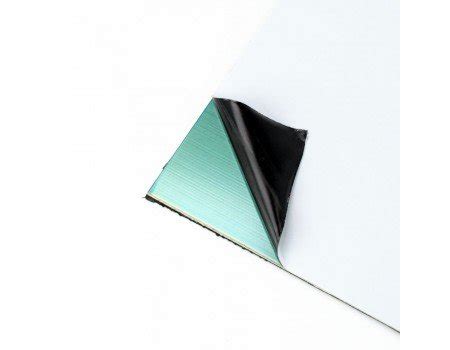
Step 3: Packaging and Storage
Once the photoresist is applied, the presensitized PCBs are packaged in light-proof containers to protect them from exposure to ambient light. The boards are typically stored in a cool, dry environment until they are ready for use.

Using Presensitized PCBs in PCB Manufacturing
Step 1: Artwork Preparation
The first step in using presensitized PCBs is to prepare the artwork for the desired circuit pattern. This artwork is typically created using PCB design software and is used to generate a photomask or film positive.
Step 2: Exposure
The presensitized PCB is placed in contact with the photomask or film positive, and the assembly is exposed to ultraviolet (UV) light. The areas of the photoresist that are exposed to UV light undergo a chemical change, making them soluble in a developing solution.
Step 3: Development
After exposure, the presensitized PCB is immersed in a developing solution, which dissolves the exposed areas of the photoresist, revealing the underlying copper layer. The unexposed areas of the photoresist remain intact, protecting the copper beneath.
Step 4: Etching
The developed presensitized PCB is then subjected to an etching process, where the exposed copper is removed using a chemical etchant. The remaining photoresist acts as a protective mask, ensuring that only the desired circuit pattern is etched into the copper layer.
Step 5: Resist Removal
After etching, the remaining photoresist is stripped away using a resist removal solution, leaving behind the finished copper circuit pattern on the PCB substrate.

Types of Presensitized PCBs
Presensitized PCBs are available in various types, each with its own characteristics and applications:
| Type | Description | Applications |
|---|---|---|
| Single-Sided | Copper layer on one side of the substrate | Simple circuits, low-cost applications |
| Double-Sided | Copper layers on both sides of the substrate | More complex circuits, improved connectivity |
| Multilayer | Multiple copper layers laminated together | High-density circuits, advanced applications |
| Flexible | Flexible substrate material (e.g., polyimide) | Wearable electronics, compact designs |
| High-Frequency | Special substrate materials (e.g., PTFE) | RF and microwave applications |

Storing and Handling Presensitized PCBs
To ensure the best performance and results when using presensitized PCBs, proper storage and handling practices are essential:
- Light Protection: Store presensitized PCBs in light-proof containers or bags to prevent accidental exposure to ambient light, which can degrade the photoresist.
- Temperature and Humidity Control: Maintain a cool, dry storage environment with a temperature range of 10-25°C (50-77°F) and a relative humidity of 40-60% to prevent moisture absorption and ensure optimal photoresist performance.
- Shelf Life: Pay attention to the shelf life of the presensitized PCBs, as the photoresist material can degrade over time. Use the boards within the specified shelf life to ensure the best results.
- Handling Precautions: When handling presensitized PCBs, wear clean gloves to avoid contaminating the photoresist surface with oils, dirt, or other debris. Minimize exposure to ambient light during handling and processing.
Troubleshooting Common Issues
Despite the advantages of presensitized PCBs, some common issues may arise during the manufacturing process. Here are a few troubleshooting tips:
Issue 1: Incomplete or Poor Resist Development
- Cause: Incorrect exposure time, weak UV light source, or expired photoresist.
- Solution: Verify the exposure time and UV light intensity, and ensure that the photoresist is within its shelf life. Adjust the exposure time or replace the UV light source if necessary.
Issue 2: Resist Adhesion Problems
- Cause: Contaminated or poorly prepared copper surface, incorrect photoresist application, or improper storage conditions.
- Solution: Clean and prepare the copper surface thoroughly before photoresist application. Verify the photoresist application process and ensure proper storage conditions.
Issue 3: Undercut or Overetched Circuit Patterns
- Cause: Overexposure, incorrect developing time, or aggressive etching process.
- Solution: Optimize the exposure and developing times, and verify the etching process parameters. Consider using a less aggressive etchant or adjusting the etching time.
Frequently Asked Questions (FAQ)
1. What is the shelf life of presensitized PCBs?
The shelf life of presensitized PCBs varies depending on the specific product and manufacturer. Typically, the shelf life ranges from 6 months to 1 year when stored under proper conditions. Always consult the manufacturer’s guidelines for specific shelf life information.
2. Can presensitized PCBs be used for both positive and negative photoresist processes?
Yes, presensitized PCBs are available with both positive and negative photoresist coatings. Positive photoresists become soluble in the developer when exposed to UV light, while negative photoresists become insoluble when exposed. The choice between positive and negative photoresists depends on the specific application and design requirements.
3. How do I select the right presensitized PCB for my project?
When selecting a presensitized PCB, consider factors such as the number of layers required, the substrate material, the desired circuit density, and any special requirements (e.g., high-frequency performance or flexibility). Consult with a PCB manufacturer or supplier to determine the best presensitized PCB option for your specific project.
4. Can presensitized PCBs be used for high-density circuit designs?
Yes, presensitized PCBs can be used for high-density circuit designs. Multilayer presensitized PCBs, in particular, are well-suited for high-density applications, as they allow for the integration of multiple copper layers and fine-pitch features. However, the achievable circuit density may be limited by the resolution of the photoresist and the capabilities of the PCB manufacturing process.
5. Are there any environmental concerns associated with the use of presensitized PCBs?
The use of presensitized PCBs does involve some environmental considerations, primarily related to the disposal of waste materials generated during the manufacturing process. These waste materials may include spent photoresist, developer, and etchant solutions, which can contain hazardous chemicals. Proper disposal and treatment of these waste materials in accordance with local regulations is essential to minimize environmental impact. Additionally, some manufacturers offer more eco-friendly presensitized PCB options, such as those that use biodegradable photoresists or less toxic developing and etching solutions.
In conclusion, presensitized PCBs offer a streamlined and efficient solution for PCB manufacturing, providing improved consistency, time savings, and cost benefits compared to traditional methods. By understanding the manufacturing process, types of presensitized PCBs, and proper storage and handling practices, designers and manufacturers can effectively leverage the advantages of this technology to create high-quality, reliable printed circuit boards for a wide range of applications.
No responses yet