Introduction to Presensitized PCBs
Presensitized PCBs, also known as photosensitive PCBs or pre-coated PCBs, are a type of printed circuit board that comes with a light-sensitive photoresist layer already applied to the copper surface. This pre-applied photoresist layer simplifies the PCB fabrication process and reduces the time and cost associated with traditional PCB manufacturing methods.
In this comprehensive article, we will explore the world of presensitized PCBs, discussing their advantages, applications, and the manufacturing process involved in creating these essential components of modern electronics.
What is a Photoresist?
To understand presensitized PCBs, it is crucial to first grasp the concept of photoresist. A photoresist is a light-sensitive material that undergoes chemical changes when exposed to ultraviolet (UV) light. There are two main types of photoresists:
-
Positive photoresist: When exposed to UV light, the exposed areas of a positive photoresist become soluble in a developer solution, while the unexposed areas remain insoluble.
-
Negative photoresist: In contrast, when a negative photoresist is exposed to UV light, the exposed areas become insoluble in the developer solution, while the unexposed areas remain soluble.
Photoresists play a vital role in the PCB fabrication process, as they allow for the selective etching of the copper layer to create the desired circuit pattern.

Advantages of Presensitized PCBs
Presensitized PCBs offer several advantages over traditional PCB manufacturing methods:
-
Time-saving: By using presensitized PCBs, manufacturers can skip the step of applying the photoresist layer, reducing the overall fabrication time.
-
Cost-effective: Presensitized PCBs eliminate the need for additional equipment and materials required for photoresist application, resulting in cost savings.
-
Consistent quality: The pre-applied photoresist layer on presensitized PCBs ensures a uniform thickness and distribution, leading to more consistent PCB quality.
-
Improved resolution: Presensitized PCBs offer better resolution and finer feature sizes compared to manually applied photoresist layers.
-
Simplified process: Using presensitized PCBs streamlines the PCB fabrication process, making it easier for manufacturers to produce high-quality boards.

Applications of Presensitized PCBs
Presensitized PCBs find applications in a wide range of industries and products, including:
-
Consumer electronics: Smartphones, tablets, laptops, and wearable devices.
-
Automotive industry: In-vehicle infotainment systems, advanced driver assistance systems (ADAS), and electric vehicle components.
-
Medical devices: Diagnostic equipment, monitoring systems, and implantable devices.
-
Industrial automation: Sensors, controllers, and communication modules.
-
Aerospace and defense: Avionics, satellite systems, and military communication equipment.
The versatility and reliability of presensitized PCBs make them an ideal choice for a broad spectrum of electronic applications.

Manufacturing Process of Presensitized PCBs
The manufacturing process of presensitized PCBs involves several key steps:
-
Substrate preparation: The PCB substrate, typically made of FR-4 or other materials, is cleaned and prepared for the application of the copper layer.
-
Copper lamination: A thin layer of copper is laminated onto the substrate using heat and pressure.
-
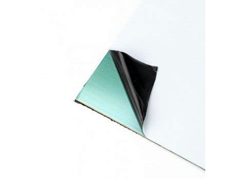
Photoresist application: The presensitized PCB comes with a pre-applied photoresist layer, eliminating the need for this step in the fabrication process.
-
Exposure: The presensitized PCB is exposed to UV light through a photomask, which contains the desired circuit pattern. The UV light causes chemical changes in the exposed areas of the photoresist.
-
Development: The exposed PCB is placed in a developer solution, which removes the soluble portions of the photoresist, revealing the copper layer beneath.
-
Etching: The PCB is submerged in an etching solution, which removes the exposed copper, leaving only the desired circuit pattern.
-
Stripping: The remaining photoresist is stripped away, leaving the final copper circuit pattern on the PCB substrate.
-
Finishing: Additional steps, such as soldermask application, silkscreen printing, and surface finish application, are performed to complete the PCB fabrication process.
By using presensitized PCBs, manufacturers can streamline this process and achieve higher quality results with greater efficiency.
Choosing the Right Presensitized PCB
When selecting a presensitized PCB for your project, consider the following factors:
-
Photoresist type: Choose between positive and negative photoresists based on your design requirements and the intended application.
-
Copper thickness: Select the appropriate copper thickness for your PCB, taking into account factors such as current carrying capacity and signal integrity.
-
Substrate material: Consider the thermal, mechanical, and electrical properties of the substrate material, such as FR-4, to ensure compatibility with your application.
-
Feature size: Evaluate the minimum feature size supported by the presensitized PCB, especially if your design requires fine pitch components or high-density interconnects.
-
Manufacturer reputation: Work with reputable PCB manufacturers who have experience in producing presensitized PCBs and can ensure consistent quality and reliability.
Troubleshooting and Best Practices
To ensure the best results when working with presensitized PCBs, keep the following troubleshooting tips and best practices in mind:
-
Storage: Store presensitized PCBs in a cool, dry place, away from direct sunlight and sources of heat or humidity, to maintain the integrity of the photoresist layer.
-
Handling: Use gloves and handle presensitized PCBs with care to avoid contamination or damage to the photoresist layer.
-
Exposure time: Ensure proper exposure time and intensity when using UV light to expose the presensitized PCB, as over- or under-exposure can lead to defects in the final circuit pattern.
-
Developer concentration: Maintain the correct concentration of the developer solution to ensure complete and accurate removal of the soluble photoresist areas.
-
Etching parameters: Control the etching process parameters, such as temperature and duration, to achieve the desired circuit pattern without over- or under-etching.
By following these best practices and troubleshooting tips, you can maximize the benefits of using presensitized PCBs in your electronic projects.
Frequently Asked Questions (FAQ)
- What is the shelf life of a presensitized PCB?
-
The shelf life of a presensitized PCB varies depending on the manufacturer and storage conditions. Typically, presensitized PCBs can last between 6 to 12 months when stored properly in a cool, dry place, away from direct sunlight and sources of heat or humidity.
-
Can presensitized PCBs be used for multilayer boards?
-
Yes, presensitized PCBs can be used for multilayer boards. The fabrication process for multilayer presensitized PCBs involves laminating multiple presensitized PCB layers together and repeating the exposure, development, and etching steps for each layer.
-
Are presensitized PCBs more expensive than traditional PCBs?
-
While the initial cost of presensitized PCBs may be slightly higher than traditional PCBs, the overall cost savings achieved through reduced fabrication time, simplified processes, and improved quality often outweigh the upfront expense.
-
Can presensitized PCBs be used for high-frequency applications?
-
Yes, presensitized PCBs can be used for high-frequency applications. By selecting the appropriate substrate material, copper thickness, and feature size, presensitized PCBs can be designed to meet the specific requirements of high-frequency applications, such as controlled impedance and signal integrity.
-
How do I select the right photoresist type for my presensitized PCB?
- The choice between positive and negative photoresists depends on your design requirements and the intended application. Positive photoresists are often preferred for designs with fine features and high resolution, while negative photoresists are better suited for applications that require high chemical resistance and durability. Consult with your PCB manufacturer to determine the best photoresist type for your specific needs.
Conclusion
Presensitized PCBs offer a range of benefits for electronic manufacturers, including time savings, cost-effectiveness, consistent quality, improved resolution, and simplified processes. By understanding the advantages, applications, and manufacturing process of presensitized PCBs, you can make informed decisions when selecting the right PCB solution for your projects.
As the electronics industry continues to evolve and demand more complex and reliable PCBs, presensitized PCBs will undoubtedly play an increasingly important role in enabling the development of innovative and high-performance electronic devices.
No responses yet