Introduction to PCB Decoupling
Proper power supply decoupling is critical for ensuring stable and reliable operation of electronic circuits on a printed circuit board (PCB). Decoupling involves strategically placing capacitors near integrated circuits (ICs) to minimize power supply noise and provide a local energy reservoir for the IC’s fast switching current demands. Without adequate decoupling, power supply noise can lead to signal integrity issues, electromagnetic interference (EMI), and even device malfunction.
In this article, we will delve into the principles behind PCB decoupling, the types of decoupling capacitors, their placement and routing techniques, and best practices for achieving effective power supply noise suppression. Whether you’re a seasoned PCB designer or just starting, understanding the intricacies of decoupling is essential for designing high-performance electronic systems.
The Need for PCB Decoupling
Sources of Power Supply Noise
Power supply noise is an unwanted voltage fluctuation on the power rails of a PCB. It can originate from various sources, including:
- Switching noise from voltage regulators
- Current transients due to IC switching activities
- Crosstalk from adjacent signal traces
- External noise coupled through power lines or EMI
These noise sources can introduce voltage ripples, spikes, or dips on the power rails, which can propagate throughout the PCB and affect the performance of sensitive components.
Impact of Power Supply Noise
Power supply noise can have several detrimental effects on electronic circuits:
- Signal integrity degradation
- Noise on the power rails can couple into signal traces, causing jitter, distortion, or false triggering.
-
It can reduce the signal-to-noise ratio (SNR) and impact the overall system performance.
-
Electromagnetic interference (EMI)
- Power supply noise can radiate electromagnetic energy, contributing to EMI and potentially violating regulatory standards.
-
It can interfere with nearby electronic devices and cause compatibility issues.
-
Device malfunction
- Excessive power supply noise can cause ICs to operate outside their specified voltage range, leading to unpredictable behavior or complete failure.
- It can trigger false resets, corrupt data, or cause intermittent system crashes.
To mitigate these issues, proper decoupling techniques must be employed to suppress power supply noise and maintain signal integrity.

Decoupling Capacitor Fundamentals
Types of Decoupling Capacitors
Decoupling capacitors come in various types and packages to cater to different frequency ranges and performance requirements. The most common types include:
- Ceramic capacitors
- Offer low equivalent series resistance (ESR) and low equivalent series inductance (ESL)
- Suitable for high-frequency decoupling (above 1 MHz)
-
Available in surface-mount device (SMD) packages like 0201, 0402, 0603, etc.
-
Tantalum capacitors
- Provide high capacitance density and good stability over temperature
- Suitable for low-frequency decoupling (below 1 MHz)
-
Available in SMD Packages and polarized
-
Electrolytic capacitors
- Offer very high capacitance values (up to several thousand microfarads)
- Suitable for bulk decoupling and low-frequency applications
-
Available in through-hole and SMD packages, polarized
-
Polymer capacitors
- Combine the advantages of ceramic and tantalum capacitors
- Offer low ESR, high capacitance density, and good temperature stability
- Suitable for a wide range of frequencies
- Available in SMD packages
The choice of decoupling capacitor depends on the specific requirements of the circuit, including the frequency range, required capacitance, and available board space.
Decoupling Capacitor Parameters
When selecting decoupling capacitors, several key parameters need to be considered:
- Capacitance
- Determines the amount of charge the capacitor can store
- Higher capacitance provides better noise suppression at lower frequencies
-
Typical values range from picofarads (pF) to microfarads (μF)
-
Equivalent Series Resistance (ESR)
- Represents the resistance of the capacitor leads and internal electrode structure
- Lower ESR enables faster charging/discharging and better high-frequency performance
-
ESR should be minimized to reduce power dissipation and improve decoupling effectiveness
-
Equivalent Series Inductance (ESL)
- Represents the inductance of the capacitor leads and internal electrode structure
- Lower ESL allows the capacitor to respond quickly to transient current demands
-
ESL should be minimized to maintain decoupling performance at high frequencies
-
Voltage Rating
- Specifies the maximum voltage the capacitor can withstand without breakdown
-
The voltage rating should be chosen based on the maximum expected voltage on the power rail, with some margin for safety
-
Temperature Coefficient
- Describes how the capacitance varies with temperature
- Stable temperature performance is important for maintaining consistent decoupling over the operating temperature range
Understanding these parameters helps in selecting the most suitable decoupling capacitors for a given application.

Decoupling Capacitor Placement and Routing
Placement Guidelines
Proper placement of decoupling capacitors is crucial for effective power supply noise suppression. The following guidelines should be considered:
- Place decoupling capacitors as close as possible to the power pins of the IC
- Minimizes the inductive path between the capacitor and the IC
-
Reduces the effective impedance seen by the IC’s power pins
-
Use multiple decoupling capacitors per IC
- Distributes the decoupling capacitance and reduces the effective inductance
-
Provides a wider frequency range of noise suppression
-
Place smaller capacitors closer to the IC and larger capacitors farther away
- Smaller capacitors (e.g., 0.1 μF) handle high-frequency noise, while larger capacitors (e.g., 10 μF) handle low-frequency noise
-
Creates a hierarchical decoupling network that covers a broad frequency spectrum
-
Consider the physical size and package of the capacitors
- Smaller packages (e.g., 0201, 0402) have lower ESL and are suitable for high-frequency decoupling
-
Larger packages (e.g., 0805, 1206) offer higher capacitance values and are suitable for low-frequency decoupling
-
Avoid placing decoupling capacitors under or near high-speed signal traces
- Minimizes the coupling of noise from the signal traces to the power plane
- Prevents the decoupling capacitors from affecting the impedance of the signal traces
Routing Techniques
Proper routing of the decoupling capacitor connections is equally important for effective noise suppression. Consider the following techniques:
- Use wide and short traces to connect the decoupling capacitors to the power and ground planes
- Minimizes the inductance and resistance of the connections
-
Ensures a low-impedance path for the high-frequency currents
-
Avoid using vias for connecting decoupling capacitors whenever possible
- Vias introduce additional inductance and can degrade high-frequency performance
-
If vias are unavoidable, use multiple vias in parallel to reduce the effective inductance
-
Maintain a clear area around the decoupling capacitors
- Avoids interference from nearby signal traces or components
-
Ensures a clean and unobstructed path for the decoupling currents
-
Use power and ground planes instead of traces whenever possible
- Planes provide a low-impedance and low-inductance path for the decoupling currents
-
Helps distribute the decoupling capacitance evenly across the PCB
-
Implement local decoupling for noise-sensitive components
- Place decoupling capacitors dedicated to specific noise-sensitive components (e.g., analog circuits, clock generators)
- Isolates the sensitive components from the noise on the main power rails
By following these placement and routing guidelines, you can optimize the effectiveness of decoupling capacitors in suppressing power supply noise.

Decoupling Capacitor Selection and Optimization
Capacitor Value Selection
Choosing the appropriate capacitance values for decoupling capacitors is an important step in the design process. Consider the following factors:
- Frequency range of the noise to be suppressed
- Select capacitor values that provide effective decoupling at the frequencies of interest
-
Use smaller capacitors (e.g., 0.01 μF to 0.1 μF) for high-frequency noise and larger capacitors (e.g., 1 μF to 10 μF) for low-frequency noise
-
Impedance profile of the decoupling capacitors
- Analyze the impedance versus frequency characteristics of the selected capacitors
-
Ensure that the combined impedance of the decoupling network is sufficiently low across the desired frequency range
-
Capacitance tolerance and variation
- Consider the tolerance and variation of the capacitance values due to manufacturing processes and temperature changes
-
Use capacitors with tighter tolerances for critical applications or compensate for variations in the design
-
Voltage rating and derating
- Select capacitors with a voltage rating higher than the maximum expected voltage on the power rail
-
Apply appropriate derating factors based on the operating conditions and reliability requirements
-
Capacitor technology and package
- Choose capacitor technology (e.g., ceramic, tantalum, polymer) based on the specific requirements of the application
- Consider the package size and footprint that can be accommodated on the PCB
Simulation and Optimization
To further optimize the decoupling network, simulation and analysis tools can be employed:
- Power integrity simulation
- Use power integrity simulation software to analyze the power distribution network (PDN) and identify potential issues
- Simulate the impact of decoupling capacitors on the PDN impedance and noise levels
-
Optimize the placement, values, and configuration of decoupling capacitors based on simulation results
-
Impedance profile analysis
- Measure or simulate the impedance versus frequency characteristics of the decoupling network
- Identify resonance points or impedance peaks that may degrade decoupling performance
-
Adjust capacitor values or add additional capacitors to flatten the impedance profile
-
Time-domain analysis
- Perform time-domain simulations to observe the transient behavior of the power supply voltage
- Analyze the voltage ripple, overshoot, and undershoot during transient events
-
Optimize the decoupling network to minimize voltage fluctuations and ensure stable operation
-
Monte Carlo analysis
- Perform Monte Carlo simulations to assess the impact of component tolerances and variations on the decoupling performance
- Identify the worst-case scenarios and ensure robust decoupling under manufacturing and environmental variations
By leveraging simulation and optimization techniques, you can fine-tune the decoupling network and achieve optimal power supply noise suppression.
PCB Layout Considerations for Decoupling
Power and Ground Plane Design
The design of power and ground planes plays a crucial role in effective decoupling. Consider the following guidelines:
- Use dedicated power and ground planes
- Assign separate layers for power and ground planes to minimize impedance and provide a low-inductance return path
-
Avoid splitting or interrupting the planes unnecessarily
-
Minimize the distance between power and ground planes
- Reduce the spacing between power and ground planes to increase the inter-plane capacitance and lower the impedance
-
Ensure adequate insulation and dielectric strength to prevent breakdown
-
Avoid narrow necks or bottlenecks in the planes
- Maintain a consistent and uninterrupted flow of current in the planes
-
Avoid creating high-impedance paths or current crowding regions
-
Use solid fills for power and ground planes
- Fill the entire plane area with copper to maximize the current-carrying capacity and minimize impedance
- Avoid hatched or crosshatched fills, as they can increase impedance and reduce decoupling effectiveness
Component Placement and Routing
Proper component placement and routing techniques can enhance the effectiveness of decoupling:
- Place decoupling capacitors close to the IC power pins
- Minimize the distance between the capacitors and the IC power pins to reduce the inductive path
-
Place the capacitors on the same layer as the IC whenever possible
-
Route power and ground traces directly to the decoupling capacitors
- Use wide and short traces to connect the decoupling capacitors to the power and ground planes
-
Avoid long and meandering traces that can increase inductance and resistance
-
Prioritize the placement of decoupling capacitors
- Place decoupling capacitors before routing other components or signal traces
-
Ensure that the decoupling capacitors have a clear and unobstructed path to the power and ground planes
-
Minimize the loop area between the capacitor and the IC
- Route the power and ground traces from the capacitor to the IC in a tight and compact manner
- Reduce the loop area to minimize the inductance and improve high-frequency decoupling
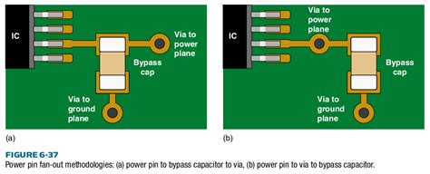
Via Optimization
Vias are necessary for connecting decoupling capacitors to power and ground planes on different layers. Optimize the via design to minimize their impact on decoupling performance:
- Use multiple vias in parallel
- Connect the decoupling capacitors to the power and ground planes using multiple vias in parallel
-
Reduces the effective inductance and improves the high-frequency decoupling
-
Place vias close to the capacitor pads
- Minimize the distance between the vias and the capacitor pads to reduce the inductive path
-
Avoid long traces between the capacitor pads and the vias
-
Use appropriate via sizes
- Choose via sizes that provide a good balance between inductance and manufacturability
-
Larger via sizes reduce inductance but may consume more board space
-
Consider via-in-pad design
- Place vias directly in the pads of the decoupling capacitors
- Eliminates the need for additional traces and reduces the inductive path
By carefully considering the PCB layout aspects, such as power and ground plane design, component placement, routing, and via optimization, you can enhance the effectiveness of decoupling and ensure robust power integrity.
Decoupling Capacitor Selection Table
The following table provides a general guide for selecting decoupling capacitors based on the frequency range and typical values:
| Frequency Range | Typical Capacitance Values |
|---|---|
| High-frequency (>100 MHz) | 0.01 μF to 0.1 μF |
| Mid-frequency (1 MHz to 100 MHz) | 0.1 μF to 1 μF |
| Low-frequency (<1 MHz) | 1 μF to 10 μF |
| Bulk decoupling | 10 μF to 100 μF |
Note that these values are approximate and may vary depending on the specific requirements of the circuit and the characteristics of the selected capacitors.
Best Practices for PCB Decoupling
To summarize, here are some best practices for effective PCB decoupling:
- Place decoupling capacitors as close as possible to the IC power pins
- Use multiple decoupling capacitors per IC to cover a wide frequency range
- Select capacitor values based on the frequency range of the noise to be suppressed
- Use ceramic capacitors for high-frequency decoupling and tantalum or electrolytic capacitors for low-frequency decoupling
- Route power and ground traces directly to the decoupling capacitors using wide and short traces
- Use dedicated power and ground planes and minimize the distance between them
- Optimize via design by using multiple vias in parallel and placing them close to the capacitor pads
- Perform power integrity simulations and impedance profile analysis to optimize the decoupling network
- Consider the PCB layout aspects, such as component placement, routing, and via optimization
- Follow the manufacturer’s recommendations and guidelines for decoupling specific ICs or devices
By adhering to these best practices and understanding the principles of PCB decoupling, you can effectively suppress power supply noise, improve signal integrity, and ensure the reliable operation of your electronic circuits.
Frequently Asked Questions (FAQ)
-
Q: What is the purpose of decoupling capacitors in PCB design?
A: Decoupling capacitors are used to suppress power supply noise and provide a stable voltage supply to integrated circuits (ICs) on a PCB. They act as local energy reservoirs, supplying the fast switching current demands of the ICs and minimizing voltage fluctuations on the power rails. -
Q: How do I determine the appropriate capacitance values for decoupling capacitors?
A: The selection of capacitance values depends on the frequency range of the noise to be suppressed. Use smaller capacitors (e.g., 0.01 μF to 0.1 μF) for high-frequency noise, larger capacitors (e.g., 1 μF to 10 μF) for low-frequency noise, and bulk capacitors (e.g., 10 μF to 100 μF) for overall stability. It’s common to use a combination of capacitors to cover a wide frequency range. -
Q: How close should decoupling capacitors be placed to the IC power pins?
A: Decoupling capacitors
No responses yet