What are SMD Packages?
SMD packages are the physical enclosures that house and protect the electronic components while providing electrical connections to the PCB. These packages come in various shapes, sizes, and pin configurations to accommodate different component types and application requirements. The choice of SMD package depends on factors such as the component’s power dissipation, pin count, and required performance characteristics.
Advantages of SMD Packages
SMD packages offer several advantages over through-hole packages:
- Smaller size: SMD packages are typically smaller than their through-hole counterparts, allowing for higher component density on the PCB.
- Lighter weight: Due to their smaller size, SMD packages contribute to overall lighter electronic devices.
- Better performance: SMD packages have shorter lead lengths, which reduces parasitic inductance and capacitance, resulting in better high-frequency performance.
- Lower cost: SMT assembly processes are highly automated, leading to lower manufacturing costs compared to through-hole assembly.
- Improved reliability: SMD packages have a stronger mechanical bond to the PCB due to their smaller size and lead pitch, resulting in improved reliability under vibration and shock conditions.

Types of SMD Packages
There are numerous types of SMD packages available, each designed for specific applications and component types. Some of the most common SMD packages include:
1. Chip Resistor and Capacitor Packages
Chip resistors and capacitors are the most basic SMD components, available in various standard sizes and values. The most common chip packages are:
0201 (0603 metric)
- Size: 0.02″ × 0.01″ (0.6mm × 0.3mm)
- Applications: High-density designs, miniature devices
0402 (1005 metric)
- Size: 0.04″ × 0.02″ (1.0mm × 0.5mm)
- Applications: General-purpose, high-density designs
0603 (1608 metric)
- Size: 0.06″ × 0.03″ (1.6mm × 0.8mm)
- Applications: General-purpose, most common size
0805 (2012 metric)
- Size: 0.08″ × 0.05″ (2.0mm × 1.25mm)
- Applications: Power circuits, higher power dissipation
1206 (3216 metric)
- Size: 0.12″ × 0.06″ (3.2mm × 1.6mm)
- Applications: Power circuits, high power dissipation
| Package | Imperial Size (in) | Metric Size (mm) | Applications |
|---|---|---|---|
| 0201 | 0.02 × 0.01 | 0.6 × 0.3 | High-density designs, miniature devices |
| 0402 | 0.04 × 0.02 | 1.0 × 0.5 | General-purpose, high-density designs |
| 0603 | 0.06 × 0.03 | 1.6 × 0.8 | General-purpose, most common size |
| 0805 | 0.08 × 0.05 | 2.0 × 1.25 | Power circuits, higher power dissipation |
| 1206 | 0.12 × 0.06 | 3.2 × 1.6 | Power circuits, high power dissipation |
2. Small Outline Packages (SOP)
Small Outline Packages (SOP) are a family of SMD packages designed for integrated circuits (ICs) with a moderate number of pins. SOPs have a rectangular body with pins on two sides, typically with a pin pitch of 0.5mm or larger. Common SOP variations include:
Small Outline Integrated Circuit (SOIC)
- Pin count: 8 to 28
- Pin pitch: 1.27mm
- Applications: General-purpose ICs, operational amplifiers, voltage regulators
Thin Small Outline Package (TSOP)
- Pin count: 8 to 56
- Pin pitch: 0.5mm to 1.27mm
- Applications: Memory devices, high-density designs
Shrink Small Outline Package (SSOP)
- Pin count: 8 to 56
- Pin pitch: 0.635mm or 0.8mm
- Applications: High-density designs, microcontrollers, sensors
Quarter-Size Small Outline Package (QSOP)
- Pin count: 8 to 100
- Pin pitch: 0.635mm or 0.8mm
- Applications: High-density designs, ASICs, mixed-signal devices
| Package | Pin Count | Pin Pitch (mm) | Applications |
|---|---|---|---|
| SOIC | 8 to 28 | 1.27 | General-purpose ICs, operational amplifiers, voltage regulators |
| TSOP | 8 to 56 | 0.5 to 1.27 | Memory devices, high-density designs |
| SSOP | 8 to 56 | 0.635 or 0.8 | High-density designs, microcontrollers, sensors |
| QSOP | 8 to 100 | 0.635 or 0.8 | High-density designs, ASICs, mixed-signal devices |
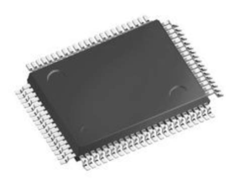
3. Quad Flat Packages (QFP)
Quad Flat Packages (QFP) are SMD packages with pins on all four sides of a square or rectangular body. QFPs are suitable for ICs with a higher pin count and are available in various sizes and pin pitches. Common QFP variations include:
Low-Profile Quad Flat Package (LQFP)
- Pin count: 32 to 256
- Pin pitch: 0.4mm to 1.0mm
- Applications: Microcontrollers, ASICs, FPGAs
Thin Quad Flat Package (TQFP)
- Pin count: 32 to 176
- Pin pitch: 0.4mm to 0.8mm
- Applications: High-density designs, microcontrollers, mixed-signal devices
Very Thin Quad Flat Package (VQFP)
- Pin count: 32 to 256
- Pin pitch: 0.4mm to 0.5mm
- Applications: High-density designs, mobile devices, wearables
| Package | Pin Count | Pin Pitch (mm) | Applications |
|---|---|---|---|
| LQFP | 32 to 256 | 0.4 to 1.0 | Microcontrollers, ASICs, FPGAs |
| TQFP | 32 to 176 | 0.4 to 0.8 | High-density designs, microcontrollers, mixed-signal devices |
| VQFP | 32 to 256 | 0.4 to 0.5 | High-density designs, mobile devices, wearables |
4. Ball Grid Array (BGA) Packages
Ball Grid Array (BGA) packages are SMD packages with a grid of solder balls underneath the package body. BGAs provide a high pin count in a compact package size, making them suitable for complex ICs and high-density designs. Common BGA variations include:
Plastic Ball Grid Array (PBGA)
- Pin count: 119 to 1089
- Pitch: 0.8mm to 1.27mm
- Applications: High-density designs, ASICs, processors
Fine-Pitch Ball Grid Array (FBGA)
- Pin count: 256 to 1156
- Pitch: 0.5mm to 0.8mm
- Applications: High-density designs, mobile devices, high-performance ICs
Wafer-Level Chip-Scale Package (WLCSP)
- Pin count: Varies
- Pitch: 0.35mm to 0.8mm
- Applications: Ultra-small devices, sensors, mobile devices
| Package | Pin Count | Pitch (mm) | Applications |
|---|---|---|---|
| PBGA | 119 to 1089 | 0.8 to 1.27 | High-density designs, ASICs, processors |
| FBGA | 256 to 1156 | 0.5 to 0.8 | High-density designs, mobile devices, high-performance ICs |
| WLCSP | Varies | 0.35 to 0.8 | Ultra-small devices, sensors, mobile devices |
5. Dual Flat No-Lead (DFN) and Quad Flat No-Lead (QFN) Packages
Dual Flat No-Lead (DFN) and Quad Flat No-Lead (QFN) packages are leadless SMD packages with exposed pads on the bottom of the package. These packages offer a smaller footprint and better thermal performance compared to leaded packages. Common DFN and QFN variations include:
Dual Flat No-Lead (DFN)
- Pin count: 6 to 16
- Body size: 2mm × 2mm to 6mm × 6mm
- Applications: Power management ICs, sensors, small-signal devices
Quad Flat No-Lead (QFN)
- Pin count: 12 to 88
- Body size: 3mm × 3mm to 12mm × 12mm
- Applications: Microcontrollers, wireless devices, power management ICs
| Package | Pin Count | Body Size (mm) | Applications |
|---|---|---|---|
| DFN | 6 to 16 | 2 × 2 to 6 × 6 | Power management ICs, sensors, small-signal devices |
| QFN | 12 to 88 | 3 × 3 to 12 × 12 | Microcontrollers, wireless devices, power management ICs |

Choosing the Right SMD Package
Selecting the appropriate SMD package for a component depends on several factors, including:
- Pin count: Choose a package that accommodates the required number of pins for the component.
- Power dissipation: Consider the package’s thermal characteristics and ensure it can handle the component’s power dissipation requirements.
- Size constraints: Select a package that fits within the available space on the PCB and meets the design’s overall size requirements.
- Performance requirements: Evaluate the package’s electrical characteristics, such as parasitic inductance and capacitance, to ensure it meets the desired performance criteria.
- Manufacturing capabilities: Ensure that the chosen package is compatible with the available SMT assembly processes and equipment.

FAQ
1. What is the difference between SMT and through-hole technology?
SMT involves mounting components directly onto the surface of a PCB, while through-hole technology requires components to be inserted into holes drilled in the PCB. SMT allows for smaller, lighter, and more efficient electronic devices.
2. Can SMD packages be soldered by hand?
Yes, SMD packages can be hand-soldered using appropriate tools and techniques. However, hand soldering becomes more challenging as the package size decreases and pin count increases. For high-volume production, automated SMT assembly processes are preferred.
3. Are SMD packages more expensive than through-hole packages?
In general, SMD packages are less expensive than their through-hole counterparts due to the higher level of automation in SMT assembly processes. However, the cost of individual components may vary depending on factors such as package size, pin count, and component complexity.
4. How do I identify the pin 1 location on an SMD package?
The pin 1 location on an SMD package is typically indicated by a dot, notch, or beveled corner on the package body. Refer to the component’s datasheet or package drawing for specific pin 1 identification details.
5. Can SMD packages be removed and replaced on a PCB?
Yes, SMD packages can be removed and replaced using specialized rework tools and techniques. However, the process can be challenging and may require skilled technicians to avoid damaging the component or the PCB. It is always best to ensure proper component selection and placement during the initial design and assembly stages.
Conclusion
Surface Mount Devices (SMDs) have become the dominant component packaging technology in the electronics industry due to their numerous advantages over through-hole packages. The wide variety of SMD packages available, such as chip resistors and capacitors, Small Outline Packages (SOP), Quad Flat Packages (QFP), Ball Grid Array (BGA) packages, and Dual Flat No-Lead (DFN) and Quad Flat No-Lead (QFN) packages, cater to diverse application requirements and design constraints.
When selecting an SMD package for a component, designers must consider factors such as pin count, power dissipation, size constraints, performance requirements, and manufacturing capabilities. By understanding the characteristics and applications of different SMD packages, designers can make informed decisions that optimize the performance, reliability, and cost-effectiveness of their electronic devices.
As electronic devices continue to evolve and become more complex, SMD packaging technologies will play a crucial role in enabling the development of smaller, lighter, and more powerful products. Staying up-to-date with the latest advancements in SMD packaging is essential for engineers and designers to create innovative and competitive electronic solutions.
No responses yet