Introduction to Microwave PCB Design
Printed Circuit Boards (PCBs) designed for microwave frequencies require special considerations to ensure optimal performance, signal integrity, and reliability. As the frequency increases, the wavelength decreases, leading to various challenges in PCB design. This article aims to provide comprehensive guidelines for designing PCBs at microwave frequencies, covering essential aspects such as material selection, layout techniques, impedance matching, and manufacturing considerations.
Understanding Microwave Frequencies
Microwave frequencies typically range from 300 MHz to 300 GHz, with wavelengths ranging from 1 meter to 1 millimeter. At these high frequencies, the electrical behavior of the PCB becomes more complex, and traditional design practices may not be sufficient. Some key characteristics of microwave frequencies include:
- Shorter wavelengths
- Higher skin effect and dielectric losses
- Increased sensitivity to impedance mismatches
- Potential for signal integrity issues, such as reflections and crosstalk

Material Selection for Microwave PCBs
Choosing the right substrate material is crucial for microwave PCB design. The material should have low dielectric loss, stable dielectric constant, and good thermal properties. Some popular substrate materials for microwave PCBs include:
| Material | Dielectric Constant (Dk) | Dissipation Factor (Df) | Thermal Conductivity (W/mK) |
|---|---|---|---|
| Rogers RO4003C | 3.38 | 0.0027 | 0.71 |
| Rogers RT/duroid 5880 | 2.20 | 0.0009 | 0.20 |
| Isola I-Tera MT40 | 3.45 | 0.0031 | 0.62 |
| Taconic RF-35 | 3.50 | 0.0018 | 0.62 |
When selecting a substrate material, consider the following factors:
– Dielectric constant and dissipation factor at the desired frequency range
– Thermal properties for heat dissipation
– Mechanical properties for manufacturing and reliability
– Cost and availability

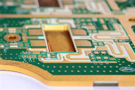
Microwave PCB Layout Techniques
Transmission Lines
At microwave frequencies, PCB traces behave as transmission lines, and their dimensions and spacing must be carefully designed to maintain the desired characteristic impedance (typically 50 ohms). The two most common types of transmission lines used in microwave PCBs are:
- Microstrip: A single conductor trace on the top layer of the PCB, with a ground plane on the bottom layer.
- Stripline: A conductor trace sandwiched between two ground planes, providing better shielding and isolation.
To calculate the dimensions of microstrip and stripline traces, use impedance calculators or simulation tools, considering the substrate material properties and the desired characteristic impedance.
Grounding and Shielding
Proper grounding and shielding are essential to minimize electromagnetic interference (EMI) and ensure signal integrity in microwave PCBs. Some guidelines for effective grounding and shielding include:
- Use a solid ground plane on the bottom layer of the PCB
- Provide sufficient ground vias near components and along transmission lines
- Use ground stitching vias to connect ground planes on different layers
- Implement shielding techniques, such as via fences or metal cans, to isolate sensitive circuitry
Component Placement and Routing
When placing components and routing traces on a microwave PCB, consider the following guidelines:
- Place components close to their associated transmission lines to minimize parasitic effects
- Avoid sharp bends or discontinuities in transmission lines, as they can cause reflections and signal distortion
- Use mitered bends or curves instead of right-angle bends to minimize impedance discontinuities
- Maintain consistent spacing between transmission lines and adjacent traces or components to avoid coupling and crosstalk

Impedance Matching Techniques
Impedance matching is crucial in microwave PCB design to minimize reflections and ensure maximum power transfer between components. Some common impedance matching techniques include:
- Series and shunt stubs: Short or open-circuited transmission line segments used to compensate for impedance mismatches.
- Tapered lines: Gradually changing the width of a transmission line to match impedances between different sections.
- Quarter-wave transformers: Transmission line segments with a specific characteristic impedance and length, used to match impedances between two different values.
When implementing impedance matching techniques, consider the bandwidth requirements and the physical space available on the PCB.
Manufacturing Considerations for Microwave PCBs
Manufacturing microwave PCBs requires specialized processes and tight tolerances to ensure the desired performance. Some key manufacturing considerations include:
- Choose a PCB fabricator with experience in high-frequency PCB manufacturing
- Specify controlled impedance requirements and provide detailed stackup information
- Use high-resolution copper etching processes to achieve precise trace widths and spacing
- Implement strict quality control measures, such as impedance testing and visual inspection
- Consider advanced packaging techniques, such as cavity-backed PCBs or chip-on-board assembly, for high-frequency components
Simulation and Testing
Simulating and testing microwave PCBs is essential to validate the design and ensure optimal performance. Some common simulation and testing methods include:
- Electromagnetic (EM) simulation: Use 3D EM simulation tools to analyze the PCB layout and identify potential issues, such as impedance mismatches or coupling.
- Network analyzer measurements: Measure the S-parameters of the PCB to characterize its frequency response, return loss, and insertion loss.
- Time-domain reflectometry (TDR): Use TDR measurements to identify impedance discontinuities and locate sources of reflections.
- Thermal analysis: Simulate and measure the thermal performance of the PCB to ensure adequate heat dissipation and reliability.
Frequently Asked Questions (FAQ)
- What is the main difference between microwave PCB design and traditional PCB design?
-
Microwave PCB design focuses on the high-frequency behavior of the PCB, taking into account factors such as transmission line effects, impedance matching, and signal integrity, which are less critical in traditional PCB design.
-
Can I use standard FR-4 substrate material for microwave PCBs?
-
While FR-4 can be used for some lower-frequency microwave applications, it is generally not recommended due to its higher dielectric loss and less stable dielectric constant at higher frequencies. It is better to use specialized substrate materials designed for microwave frequencies, such as Rogers or Taconic materials.
-
What is the importance of grounding in microwave PCB design?
-
Proper grounding is crucial in microwave PCB design to provide a low-impedance return path for high-frequency currents, minimize EMI, and ensure signal integrity. A solid ground plane and sufficient ground vias are essential for effective grounding.
-
How can I minimize crosstalk between transmission lines on a microwave PCB?
-
To minimize crosstalk, maintain adequate spacing between transmission lines, use ground planes to provide shielding, and consider using stripline structures instead of microstrip for better isolation. Additionally, use simulation tools to analyze the coupling between transmission lines and optimize the layout accordingly.
-
What are the challenges in manufacturing microwave PCBs?
- Manufacturing microwave PCBs requires tight tolerances, high-resolution copper etching, and specialized processes to achieve the desired performance. Challenges include maintaining consistent impedance control, minimizing fabrication variations, and ensuring reliable connections for high-frequency components. Working with experienced PCB fabricators and implementing strict quality control measures are essential for successful manufacturing of microwave PCBs.
Conclusion
Designing PCBs for microwave frequencies presents unique challenges and requires careful consideration of various factors, such as material selection, layout techniques, impedance matching, and manufacturing processes. By following the guidelines outlined in this article and utilizing simulation and testing methods, designers can create reliable and high-performance microwave PCBs.
As the demand for high-frequency applications continues to grow, staying up-to-date with the latest advancements in microwave PCB design techniques and technologies is crucial. Continuous learning, collaboration with experienced professionals, and staying engaged with the microwave engineering community will help designers stay ahead of the curve and tackle the challenges of designing PCBs at microwave frequencies.
No responses yet