Introduction to PCB and PCBA
Printed Circuit Boards (PCBs) and Printed Circuit Board Assemblies (PCBAs) are essential components in modern electronics. While these terms are often used interchangeably, they refer to different stages in the manufacturing process of electronic devices. Understanding the difference between PCB and PCBA is crucial for anyone involved in electronics design, manufacturing, or procurement.
What is a PCB?
A PCB is a flat board made of insulating materials, such as fiberglass or composite epoxy, with conductive copper traces printed on its surface. These traces connect various electronic components, such as resistors, capacitors, and integrated circuits (ICs), to form a complete circuit. PCBs provide a stable and organized platform for mounting and interconnecting electronic components, ensuring reliable performance and compact design.
What is a PCBA?
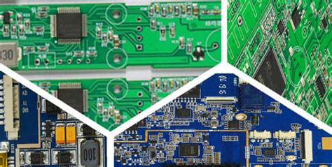
A PCBA, on the other hand, is a PCB with all the necessary electronic components mounted and soldered onto it. It is the final product that results from the assembly process, which involves placing components on the PCB, soldering them in place, and testing the completed assembly for functionality. A PCBA is a fully functional circuit board ready to be integrated into an electronic device.
The PCB Manufacturing Process
The PCB manufacturing process involves several steps that transform a design concept into a physical board. These steps include:
-
Design: The PCB design is created using specialized software, such as Altium Designer or Eagle. The design includes the component layout, trace routing, and any necessary mechanical features.
-
Printing: The PCB design is printed onto a copper-clad laminate using a photoresist process. The exposed areas of the copper are etched away, leaving behind the desired trace pattern.
-
Drilling: Holes are drilled into the PCB to accommodate through-hole components and provide interconnections between layers in multi-layer boards.
-
Plating: The drilled holes are plated with copper to ensure electrical conductivity and to protect the exposed surfaces from oxidation.
-
Solder Mask Application: A layer of solder mask is applied to the PCB surface to protect the copper traces from short circuits and to provide insulation.
-
Silkscreen Printing: Text, logos, and component designators are printed onto the PCB surface using a silkscreen process, making it easier to identify components during assembly and troubleshooting.
| Step | Description |
|---|---|
| Design | PCB design created using specialized software |
| Printing | Design printed onto copper-clad laminate |
| Drilling | Holes drilled for through-hole components and interconnections |
| Plating | Drilled holes plated with copper for conductivity and protection |
| Solder Mask Application | Solder mask layer applied for insulation and short circuit prevention |
| Silkscreen Printing | Text, logos, and component designators printed for easy identification |

The PCBA Assembly Process
Once the PCB manufacturing process is complete, the PCBA assembly process begins. This process involves several steps:
-
Solder Paste Application: Solder paste, a mixture of tiny solder particles and flux, is applied to the PCB’s surface where components will be placed. This is typically done using a stencil and a solder paste printer.
-
Component Placement: Surface mount components are placed onto the solder paste using a pick-and-place machine. Through-hole components are inserted manually or with the help of automation.
-
Reflow Soldering: The PCB with the placed components is passed through a reflow oven, which melts the solder paste, forming a permanent connection between the components and the PCB.
-
Inspection: The assembLED PCBA undergoes visual and automated optical inspection (AOI) to ensure that all components are correctly placed and soldered.
-
Testing: Functional testing is performed on the PCBA to verify that it meets the required specifications and performs as intended.
-
Conformal Coating (Optional): In some cases, a conformal coating is applied to the PCBA to protect it from environmental factors such as moisture, dust, and chemicals.
| Step | Description |
|---|---|
| Solder Paste Application | Solder paste applied to PCB surface using stencil and printer |
| Component Placement | Surface mount components placed using pick-and-place machine, through-hole components inserted manually or with automation |
| Reflow Soldering | PCB with components passed through reflow oven to melt solder paste and form permanent connections |
| Inspection | Assembled PCBA undergoes visual and automated optical inspection to ensure correct placement and soldering |
| Testing | Functional testing performed to verify PCBA meets specifications and performs as intended |
| Conformal Coating (Optional) | Conformal coating applied to protect PCBA from environmental factors |

Differences between PCB and PCBA
While PCBs and PCBAs are closely related, there are several key differences between them:
-
Components: A PCB is a bare board without any electronic components mounted on it, while a PCBA has all the necessary components soldered onto the board.
-
Functionality: A PCB is not functional on its own, as it requires the addition of electronic components to form a complete circuit. A PCBA, on the other hand, is a fully functional circuit board ready to be integrated into an electronic device.
-
Manufacturing Process: The PCB manufacturing process involves designing, printing, drilling, plating, and applying solder mask and silkscreen. The PCBA assembly process builds upon the PCB, adding steps such as solder paste application, component placement, reflow soldering, inspection, and testing.
-
Cost: PCBs are generally less expensive than PCBAs, as they do not include the cost of components and the assembly process.
-
Lead Time: PCBs typically have a shorter lead time compared to PCBAs, as the assembly process can be time-consuming, especially for complex designs with many components.
| Factor | PCB | PCBA |
|---|---|---|
| Components | Bare board without components | Board with components soldered |
| Functionality | Not functional on its own | Fully functional circuit board |
| Manufacturing Process | Designing, printing, drilling, plating, solder mask, and silkscreen | Includes PCB process plus solder paste application, component placement, reflow soldering, inspection, and testing |
| Cost | Less expensive | More expensive due to components and assembly |
| Lead Time | Shorter lead time | Longer lead time due to assembly process |

Applications of PCBs and PCBAs
PCBs and PCBAs are used in a wide range of electronic devices and industries, including:
-
Consumer Electronics: Smartphones, tablets, laptops, televisions, and home appliances.
-
Automotive: Engine control units, infotainment systems, and advanced driver assistance systems (ADAS).
-
Medical Devices: Patient monitors, diagnostic equipment, and implantable devices.
-
Industrial Automation: Programmable logic controllers (PLCs), sensors, and motor drives.
-
Aerospace and Defense: Avionics, communication systems, and military equipment.
Advantages of using PCBs and PCBAs
Using PCBs and PCBAs in electronic devices offers several advantages:
-
Compact Design: PCBs allow for the compact arrangement of electronic components, reducing the overall size of the device.
-
Reliability: PCBs provide a stable and durable platform for electronic components, ensuring reliable performance and reducing the risk of failures.
-
Standardization: PCBs and PCBAs are designed and manufactured according to industry standards, making it easier to ensure compatibility and interchangeability between different devices and manufacturers.
-
Automated Manufacturing: The PCB and PCBA Manufacturing processes are highly automated, enabling high-volume production and consistent quality.
-
Cost-effective: PCBs and PCBAs are cost-effective solutions for mass-produced electronic devices, as they reduce the need for manual wiring and assembly.
Choosing between PCB and PCBA
When deciding between PCB and PCBA, consider the following factors:
-
Project Requirements: If you need a fully functional circuit board, a PCBA is the appropriate choice. If you only require the bare board for custom assembly or testing, a PCB may suffice.
-
In-house Capabilities: If your organization has the necessary equipment and expertise to assemble PCBs, you may opt to purchase PCBs and perform the assembly in-house. Otherwise, outsourcing the assembly process to a PCBA manufacturer may be more practical.
-
Time-to-Market: If you have a tight deadline, opting for a PCBA may be faster, as the manufacturer can handle both the PCB fabrication and assembly processes.
-
Cost: PCBs are generally less expensive than PCBAs, but the total cost of ownership should be considered, including the cost of components, assembly, and testing.
Future Trends in PCB and PCBA Technology
As electronic devices continue to evolve, so do PCB and PCBA technologies. Some of the current and future trends include:
-
Miniaturization: The demand for smaller, more compact electronic devices is driving the development of advanced PCB technologies, such as high-density interconnect (HDI) and embedded component PCBs.
-
Flexible and Stretchable PCBs: Flexible and stretchable PCBs are gaining popularity in wearable devices, medical applications, and IoT sensors, enabling the creation of more versatile and adaptable electronic products.
-
3D Printing: The use of 3D printing technologies in PCB manufacturing is expected to grow, allowing for the rapid prototyping and production of complex PCB designs.
-
Advanced Materials: New materials, such as graphene and carbon nanotubes, are being explored for use in PCBs, offering the potential for improved thermal management, electrical performance, and mechanical strength.
-
Sustainable Manufacturing: There is a growing focus on environmentally friendly PCB and PCBA manufacturing processes, including the use of lead-free solders, recyclable materials, and energy-efficient equipment.
Frequently Asked Questions (FAQ)
-
Q: Can a PCB function without components?
A: No, a PCB is not functional on its own. It requires the addition of electronic components to form a complete circuit and perform its intended function. -
Q: Is it possible to assemble a PCBA manually?
A: Yes, it is possible to assemble a PCBA manually, especially for low-volume production or prototyping. However, manual assembly is time-consuming and may result in a higher risk of errors compared to automated assembly processes. -
Q: What is the difference between surface mount and through-hole components?
A: Surface mount components are placed directly onto the surface of the PCB and soldered in place, while through-hole components have leads that are inserted into holes drilled in the PCB and soldered on the opposite side. Surface mount components are generally smaller and more suitable for high-density designs, while through-hole components offer better mechanical stability. -
Q: Can a PCBA be repaired if a component fails?
A: Yes, a PCBA can be repaired by replacing the faulty component. However, the ease of repair depends on factors such as the component type, the PCB design, and the accessibility of the faulty component. In some cases, it may be more cost-effective to replace the entire PCBA rather than repair it. -
Q: What is the typical turnaround time for PCB and PCBA manufacturing?
A: The turnaround time for PCB and PCBA manufacturing varies depending on factors such as the complexity of the design, the number of layers, the quantity ordered, and the manufacturer’s workload. Generally, PCBs can be manufactured within 1-2 weeks, while PCBAs may take 2-4 weeks or longer, depending on the assembly requirements and testing procedures.
Conclusion
Understanding the difference between PCB and PCBA is essential for anyone involved in the design, manufacturing, or procurement of electronic devices. While PCBs provide the foundation for electronic circuits, PCBAs are the fully assembled and functional circuit boards ready for integration into electronic products.
The choice between PCB and PCBA depends on various factors, including project requirements, in-house capabilities, time-to-market, and cost. As electronic devices continue to evolve, so do PCB and PCBA technologies, with trends such as miniaturization, flexible and stretchable PCBs, 3D printing, advanced materials, and sustainable manufacturing shaping the future of the industry.
By staying informed about the differences between PCB and PCBA and the latest industry trends, professionals in the electronics field can make informed decisions and create innovative, reliable, and cost-effective electronic products.
No responses yet