Introduction to PCB Transmission Lines
In the world of electronics, the Printed Circuit Board (PCB) is a fundamental component that enables the interconnection and functionality of various electronic devices. One of the critical aspects of PCB design is the transmission line, which plays a vital role in ensuring the proper transfer of signals between transmitters and receivers. This article delves into the intricacies of PCB transmission lines, exploring their significance, types, design considerations, and best practices for optimal performance.
What is a PCB Transmission Line?
A PCB transmission line is a specialized trace or pathway on a PCB that is designed to carry high-frequency signals between components. Unlike regular traces, which are primarily concerned with connectivity, transmission lines are engineered to maintain signal integrity and minimize signal distortion. They are crucial in applications where signal quality and timing are of utmost importance, such as in high-speed digital circuits, radio frequency (RF) systems, and telecommunications equipment.
The Importance of PCB Transmission Lines
In modern electronics, the demand for faster data transfer rates and higher signal frequencies has made PCB transmission lines indispensable. As signal frequencies increase, the wavelengths of the signals become shorter, making them more susceptible to various signal integrity issues. These issues can include reflections, crosstalk, and electromagnetic interference (EMI), which can degrade signal quality and lead to system malfunction.
PCB transmission lines address these challenges by providing a controlled environment for signal propagation. By carefully designing the geometry and material properties of the transmission line, engineers can minimize signal distortion, ensure proper impedance matching, and maintain signal integrity across the PCB.
Types of PCB Transmission Lines
There are several types of PCB transmission lines, each with its own characteristics and applications. The choice of transmission line depends on factors such as the frequency range, signal power, and the specific requirements of the circuit. Let’s explore some of the most common types of PCB transmission lines.
Microstrip Transmission Lines
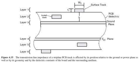
Microstrip transmission lines are one of the most widely used types of PCB transmission lines. They consist of a conductive trace on the top layer of the PCB, with a ground plane on the bottom layer. The dielectric material of the PCB substrate separates the trace from the ground plane.
Microstrip transmission lines offer several advantages, including:
– Easy fabrication and integration with other components
– Good impedance control and matching
– Relatively low cost compared to other Transmission Line Types
However, microstrip lines also have some limitations:
– Higher radiation losses compared to other transmission line types
– Susceptible to crosstalk and EMI due to the exposed trace
– Limited power handling capability
Stripline Transmission Lines
Stripline transmission lines are another popular choice for PCB designers. In a stripline configuration, the conductive trace is sandwiched between two ground planes, with dielectric material on both sides. This arrangement provides a shielded environment for the signal, reducing radiation losses and minimizing crosstalk and EMI.
Stripline transmission lines offer several benefits:
– Excellent isolation and shielding from external interference
– Low radiation losses
– Good power handling capability
However, stripline transmission lines also have some drawbacks:
– More complex fabrication process compared to microstrip lines
– Increased PCB thickness due to the additional layers
– Limited access to the signal trace for probing or debugging
Coplanar Waveguide (CPW) Transmission Lines
Coplanar waveguide (CPW) transmission lines consist of a conductive trace with ground planes on either side, all on the same layer of the PCB. The signal trace and ground planes are separated by a gap, which is filled with the dielectric material of the PCB substrate.
CPW transmission lines offer several advantages:
– Easy integration with surface-mounted components
– Good isolation and shielding properties
– Reduced dispersion compared to microstrip lines
However, CPW transmission lines also have some limitations:
– Higher manufacturing complexity compared to microstrip lines
– Increased PCB area consumption due to the additional ground planes
– Potential for Mode Conversion and signal leakage

PCB Transmission Line Design Considerations
Designing PCB transmission lines requires careful consideration of various factors to ensure optimal signal integrity and performance. Let’s explore some of the key design considerations for PCB transmission lines.
Characteristic Impedance
Characteristic impedance is a fundamental property of a transmission line that determines how signals propagate along the line. It is determined by the geometry and material properties of the transmission line, such as the width and thickness of the trace, the dielectric constant of the substrate, and the spacing between the trace and ground plane.
Matching the characteristic impedance of the transmission line to the impedance of the source and load is crucial for minimizing reflections and ensuring efficient power transfer. Common characteristic impedance values for PCB transmission lines include 50 ohms, 75 ohms, and 100 ohms, depending on the application.
Dielectric Material Selection
The choice of dielectric material for the PCB substrate plays a significant role in the performance of transmission lines. The dielectric constant (Dk) and dissipation factor (Df) of the material determine the speed of signal propagation and the amount of signal loss, respectively.
For high-speed applications, materials with low Dk and Df values are preferred to minimize Signal Delay and attenuation. Common dielectric materials used in PCB transmission lines include FR-4, Rogers, and Teflon.
Trace Geometry
The geometry of the transmission line trace, including its width, thickness, and spacing from other traces and ground planes, directly affects its characteristic impedance and signal integrity. Wider traces have lower impedance and can handle higher currents, while narrower traces have higher impedance and are more susceptible to manufacturing variability.
The thickness of the trace also influences its current-carrying capacity and high-frequency performance. Thicker traces have lower resistance and can handle higher currents, but they may also introduce unwanted inductance and capacitance effects at high frequencies.
Length Matching
In high-speed digital systems, it is essential to match the lengths of transmission lines that carry signals between components. Length mismatches can introduce timing skew and degrade signal integrity, leading to data errors and system malfunction.
Length matching techniques, such as serpentine routing and delay lines, can be used to equalize the electrical lengths of transmission lines and ensure synchronous arrival of signals at their destinations.
Termination Techniques
Proper termination of transmission lines is crucial for preventing signal reflections and maintaining signal integrity. Reflections occur when a signal encounters an impedance mismatch at the end of the transmission line, causing a portion of the signal to be reflected back towards the source.
Termination techniques, such as Series termination, parallel termination, and AC termination, can be used to match the impedance of the transmission line to the load and minimize reflections. The choice of termination technique depends on factors such as the signal frequency, power consumption, and available PCB space.

Best Practices for PCB Transmission Line Design
To ensure optimal performance and signal integrity in PCB transmission lines, designers should follow some best practices:
- Use controlled impedance design techniques to match the characteristic impedance of the transmission line to the source and load impedances.
- Choose appropriate dielectric materials based on the frequency range and signal speed requirements of the application.
- Minimize the length of transmission lines to reduce signal delay and attenuation.
- Use length matching techniques to ensure synchronous arrival of signals at their destinations.
- Implement proper termination techniques to minimize signal reflections and maintain signal integrity.
- Follow manufacturer guidelines and industry standards for trace geometry, spacing, and routing.
- Perform signal integrity simulations and analysis to validate the design and identify potential issues before fabrication.
- Use ground planes and shielding techniques to minimize crosstalk and EMI.
- Consider the effect of vias and layer transitions on the transmission line performance and use appropriate compensation techniques.
- Collaborate with PCB fabricators and assembly providers to ensure manufacturability and reliability of the transmission line design.

Conclusion
PCB transmission lines are essential components in modern electronic systems, enabling the reliable transfer of high-frequency signals between transmitters and receivers. By understanding the types of transmission lines, design considerations, and best practices, engineers can create robust and high-performance PCB designs that meet the demanding requirements of today’s applications.
As signal frequencies continue to increase and system complexity grows, the importance of well-designed PCB transmission lines will only become more significant. By staying abreast of the latest advancements in materials, design techniques, and simulation tools, designers can overcome the challenges associated with high-speed signal propagation and ensure the success of their electronic products.
Frequently Asked Questions (FAQ)
- What is the difference between a microstrip and a stripline transmission line?
-
A microstrip transmission line has a conductive trace on the top layer of the PCB, with a ground plane on the bottom layer. In contrast, a stripline transmission line has the conductive trace sandwiched between two ground planes, providing better shielding and isolation.
-
How does the dielectric material affect the performance of a PCB transmission line?
-
The dielectric material determines the speed of signal propagation (through its dielectric constant, Dk) and the amount of signal loss (through its dissipation factor, Df). Materials with low Dk and Df values are preferred for high-speed applications to minimize signal delay and attenuation.
-
Why is impedance matching important in PCB transmission line design?
-
Impedance matching is crucial for minimizing signal reflections and ensuring efficient power transfer. When the characteristic impedance of the transmission line matches the impedance of the source and load, reflections are minimized, and signal integrity is maintained.
-
What are some common termination techniques used in PCB transmission lines?
-
Common termination techniques include series termination (adding a resistor in series with the source), parallel termination (adding a resistor in parallel with the load), and AC termination (using a capacitor to provide a high-frequency path to ground). The choice of termination technique depends on factors such as the signal frequency, power consumption, and available PCB space.
-
How can designers minimize crosstalk and EMI in PCB transmission lines?
- Designers can minimize crosstalk and EMI by using ground planes and shielding techniques, such as placing ground traces between signal traces or using guard traces. Proper spacing between traces and ground planes, as well as the use of differential signaling, can also help reduce crosstalk and EMI.
| Transmission Line Type | Advantages | Disadvantages |
|---|---|---|
| Microstrip | – Easy fabrication and integration – Good impedance control and matching – Relatively low cost |
– Higher radiation losses – Susceptible to crosstalk and EMI – Limited power handling capability |
| Stripline | – Excellent isolation and shielding – Low radiation losses – Good power handling capability |
– More complex fabrication process – Increased PCB thickness – Limited access to the signal trace |
| Coplanar Waveguide | – Easy integration with surface-mounted components – Good isolation and shielding – Reduced dispersion |
– Higher manufacturing complexity – Increased PCB area consumption – Potential for mode conversion and signal leakage |

No responses yet