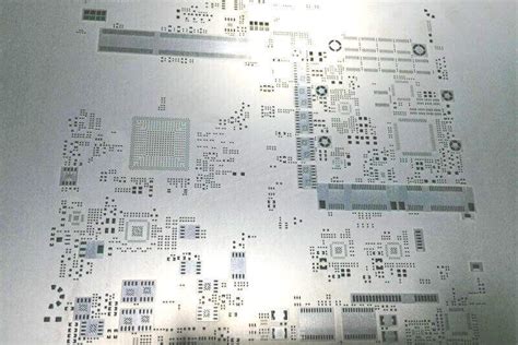
What are PCB Stencils?
PCB stencils, also known as solder paste stencils, are thin metal sheets with cut-outs that match the pads on a printed circuit board (PCB). They are used to apply solder paste onto the PCB pads before component placement and soldering. The stencil ensures that the right amount of solder paste is applied to each pad, resulting in a consistent and reliable solder joint.
Types of PCB Stencils
There are two main types of PCB stencils:
-
Framed Stencils: These stencils have a metal frame around the perimeter, which provides stability and rigidity. They are easier to handle and align with the PCB.
-
Frameless Stencils: These stencils do not have a metal frame and are typically thinner than framed stencils. They are more flexible and can conform to slight variations in PCB Thickness.
PCB Stencil Materials
PCB stencils can be made from various materials, each with its own advantages and disadvantages:
| Material | Advantages | Disadvantages |
|---|---|---|
| Stainless Steel | Durable, long lifespan, suitable for high-volume production | Expensive, not suitable for fine-pitch applications |
| Nickel | Good durability, less expensive than stainless steel | Not as durable as stainless steel, may warp over time |
| Polyimide | Suitable for fine-pitch applications, less expensive than metal stencils | Less durable, may require frequent replacement |
How to Make PCB Stencils
Step 1: Prepare the PCB Design
Before creating a PCB stencil, you need to have a finalized PCB design. Ensure that the design has been thoroughly checked for errors and that all the pads are correctly sized and spaced.
Step 2: Generate Stencil Gerber Files
Most PCB design software can generate Gerber files specifically for stencil fabrication. These files contain the information needed to cut the stencil, including the pad sizes, locations, and aperture shapes.
To generate stencil Gerber files:
- Open your PCB design software and load the PCB design file.
- Select the layer(s) containing the pads for which you want to create a stencil.
- Set the aperture size and shape for each pad. The aperture should be slightly smaller than the pad size to prevent solder paste from spreading beyond the pad edges.
- Generate the Gerber files for the selected layer(s). Make sure to choose the appropriate settings for stencil fabrication, such as the file format and units.
Step 3: Choose a Stencil Fabrication Method
There are several methods for fabricating PCB stencils, each with its own advantages and limitations:
Laser Cutting
Laser cutting uses a high-powered laser to cut the stencil apertures. This method is suitable for both framed and frameless stencils and can achieve high precision and accuracy. However, laser cutting can be expensive, especially for small quantities.
Chemical Etching
Chemical etching involves applying a photoresist to the stencil material, exposing it to UV light through a photomask, and then etching away the unwanted areas with a chemical solution. This method is less expensive than laser cutting but may not achieve the same level of precision.
Electroforming
Electroforming is a process that uses electroplating to create a stencil from a master pattern. This method can produce high-quality stencils with fine features but is typically more expensive and time-consuming than other methods.
Step 4: Send Gerber Files to Stencil Manufacturer
Once you have generated the stencil Gerber files and chosen a fabrication method, send the files to a stencil manufacturer. Many PCB fabrication services also offer stencil manufacturing, or you can use a dedicated stencil manufacturer.
When ordering your stencil, specify the following:
- Stencil material
- Stencil thickness
- Framed or frameless
- Quantity
- Delivery requirements
Step 5: Inspect and Test the Stencil
Upon receiving your PCB stencil, inspect it for any defects or inconsistencies. Check that the apertures are correctly sized and shaped and that there are no signs of damage or contamination.
Before using the stencil for production, test it on a sample PCB to ensure that it applies the solder paste correctly. If there are any issues, contact the stencil manufacturer for a replacement or revision.

Tips for Successful PCB Stencil Use
-
Keep the stencil clean: Always clean the stencil before and after use to prevent solder paste buildup and contamination. Use a stencil cleaner or isopropyl alcohol and a lint-free cloth.
-
Secure the stencil: When using the stencil, ensure that it is securely aligned with the PCB and held in place. Use a stencil frame or clamps to prevent shifting or warping.
-
Control solder paste volume: The amount of solder paste applied to each pad depends on the stencil thickness and aperture size. Use the appropriate thickness and aperture dimensions for your specific application.
-
Store the stencil properly: When not in use, store the stencil in a protective case or bag to prevent damage and contamination. Avoid exposing the stencil to extreme temperatures or humidity.

FAQ
- What is the recommended stencil thickness for SMT components?
-
The recommended stencil thickness depends on the component size and pitch. For most standard SMT components, a stencil thickness of 0.1 mm to 0.15 mm is suitable. For fine-pitch components or smaller pads, a thinner stencil (0.08 mm to 0.1 mm) may be necessary.
-
Can I reuse a PCB stencil?
-
Yes, PCB stencils can be reused multiple times if they are properly cleaned and stored after each use. However, over time, the stencil may wear out or become damaged, affecting the solder paste application quality. It’s essential to inspect the stencil regularly and replace it when necessary.
-
How do I align the stencil with the PCB?
-
Most stencils have fiducial marks or alignment holes that correspond to similar marks or holes on the PCB. By aligning these marks, you can ensure that the stencil is correctly positioned on the PCB. Some stencil frames also have adjustable pins or clamps that help secure the stencil in place.
-
What is the difference between a stepped stencil and a standard stencil?
-
A stepped stencil has different thicknesses for different areas of the PCB, allowing for varying solder paste volumes. This is useful when a PCB has components with different sizes or heights. A standard stencil has a uniform thickness across the entire stencil.
-
Can I make my own PCB stencil?
- While it is possible to make your own PCB stencil, it requires specialized equipment and expertise. For most applications, it is more cost-effective and time-efficient to outsource stencil fabrication to a professional manufacturer. However, if you have the necessary resources and skills, you can create your own stencils using methods such as laser cutting or chemical etching.

Conclusion
PCB stencils are an essential tool for applying solder paste accurately and consistently during the PCB Assembly process. By understanding the different types of stencils, materials, and fabrication methods, you can choose the best stencil for your specific application.
To make a PCB stencil, start by preparing your PCB design and generating stencil Gerber files. Choose a suitable fabrication method and send the files to a stencil manufacturer. Upon receiving the stencil, inspect it for quality and test it before using it in production.
By following best practices for stencil use and maintenance, you can ensure reliable and high-quality solder paste application, leading to better PCB assembly results.
No responses yet