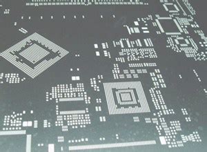
What are PCB Stencils?
PCB stencils, also known as solder paste stencils, are thin metal sheets with precise openings that correspond to the pads on a printed circuit board (PCB). These stencils are used during the PCB Assembly process to apply solder paste onto the pads, ensuring accurate and consistent placement of components.
Types of PCB Stencils
There are several types of PCB stencils available, each with its own advantages and disadvantages. The most common types include:
| Type | Description | Advantages | Disadvantages |
|---|---|---|---|
| Laser-cut | Made using a laser to cut openings in a metal sheet | High precision, durable, suitable for fine-pitch components | Expensive, longer lead times |
| Chemical-etched | Created by chemically etching the metal sheet | Cost-effective, faster lead times | Lower precision compared to laser-cut stencils |
| Electroformed | Produced by electroplating nickel onto a master template | Extremely high precision, suitable for ultra-fine pitch components | Most expensive, longer lead times |
The Importance of PCB Stencils in PCB Fabrication
Ensuring Precise Solder Paste Application
One of the most crucial roles of PCB stencils is to ensure precise solder paste application onto the PCB pads. The stencil’s openings are designed to match the exact dimensions and locations of the pads, allowing for the correct amount of solder paste to be deposited. This precision is essential for several reasons:
- Proper component placement: Accurate solder paste application ensures that components are placed correctly on the pads, reducing the risk of misalignment or bridging.
- Optimal solder joint formation: The right amount of solder paste is necessary for creating strong and reliable solder joints between the components and the PCB.
- Minimizing defects: Precise solder paste application helps minimize common defects such as solder bridges, insufficient solder, or tombstoning.
Improving Production Efficiency
PCB stencils play a vital role in improving the efficiency of the PCB assembly process. By using stencils, manufacturers can:
- Accelerate the solder paste application process: Stencils allow for quick and uniform application of solder paste across the entire PCB, reducing the time required for this step.
- Enable automated assembly: Stencils are compatible with automated solder paste printing machines, which further increases the speed and consistency of the assembly process.
- Reduce manual intervention: Stencils minimize the need for manual solder paste application, reducing the risk of human error and ensuring a more consistent output.
Accommodating Diverse Component Sizes and Types
As electronic devices become more compact and complex, PCBs need to accommodate a wide range of component sizes and types. PCB stencils are essential for handling this diversity:
- Fine-pitch components: Stencils with high-precision openings enable the accurate application of solder paste for fine-pitch components, such as ball grid arrays (BGAs) or quad flat no-lead (QFN) packages.
- Varied pad sizes: Stencils can be designed with openings of different sizes to accommodate varying pad dimensions on a single PCB.
- Mixed technology boards: Stencils enable the assembly of PCBs with a mix of through-hole and surface-mount components by selectively applying solder paste to the appropriate pads.

Stencil Design Considerations
To ensure optimal performance, several factors must be considered when designing PCB stencils:
Aperture Size and Shape
The size and shape of the stencil openings, or apertures, directly impact the solder paste deposit on the PCB pads. Some key considerations include:
- Aperture width: The width of the aperture should be slightly larger than the pad width to allow for proper solder paste release.
- Aperture length: The length of the aperture should be long enough to accommodate the desired solder paste volume but short enough to prevent bridging.
- Aperture shape: The shape of the aperture can be circular, square, or rectangular, depending on the pad geometry and the desired solder paste deposit profile.
Stencil Thickness
The thickness of the PCB stencil determines the volume of solder paste deposited on the pads. Factors to consider when selecting stencil thickness include:
- Component type: Smaller, fine-pitch components require thinner stencils (typically 0.1-0.15mm), while larger components can accommodate thicker stencils (0.2-0.3mm).
- Solder paste properties: The viscosity and particle size of the solder paste should be considered when choosing the stencil thickness to ensure proper release and flow.
- PCB design: The overall design of the PCB, including pad size and spacing, should be factored in when determining the appropriate stencil thickness.
Stencil Material
The choice of stencil material affects its durability, performance, and cost. Common materials include:
- Stainless steel: Durable and suitable for high-volume production, but more expensive than other options.
- Nickel: Offers excellent durability and is resistant to wear, but is more costly than stainless steel.
- Polyester: A cost-effective option for low-volume or prototype production, but has a shorter lifespan compared to metal stencils.

Stencil Maintenance and Handling
Proper maintenance and handling of PCB stencils are essential for ensuring consistent performance and longevity. Some best practices include:
- Regular cleaning: Stencils should be cleaned regularly to remove solder paste residue and prevent clogging of the apertures. Cleaning can be done using solvents or ultrasonic cleaners.
- Inspection: Stencils should be inspected periodically for signs of wear, damage, or clogging. Damaged or worn stencils should be replaced to maintain print quality.
- Storage: When not in use, stencils should be stored in a clean, dry environment to prevent contamination and damage. Stencils should be stored flat or hung vertically to avoid warping.

Frequently Asked Questions (FAQ)
1. What is the difference between a solder paste stencil and a solder mask?
A solder paste stencil is a thin metal sheet with openings that correspond to the pads on a PCB, used to apply solder paste during the assembly process. A solder mask, on the other hand, is a layer applied to the PCB surface to protect the copper traces and prevent solder bridging.
2. Can PCB stencils be reused?
Yes, PCB stencils can be reused multiple times if properly cleaned and maintained. However, over time, stencils may wear out or become damaged, requiring replacement to maintain print quality.
3. How do I choose the right stencil thickness for my PCB?
The choice of stencil thickness depends on factors such as component type, solder paste properties, and PCB design. As a general guideline, thinner stencils (0.1-0.15mm) are used for smaller, fine-pitch components, while thicker stencils (0.2-0.3mm) are used for larger components.
4. What is the typical lifespan of a PCB stencil?
The lifespan of a PCB stencil varies depending on factors such as material, usage, and maintenance. Metal stencils (stainless steel or nickel) can last for thousands of prints if properly cared for, while polyester stencils have a shorter lifespan and are better suited for low-volume or prototype production.
5. Can PCB stencils be customized for specific PCB designs?
Yes, PCB stencils are custom-made for each specific PCB design. The stencil apertures are created based on the size, shape, and location of the pads on the PCB, ensuring precise solder paste application.
Conclusion
PCB stencils play a critical role in the PCB fabrication process, ensuring precise solder paste application, improving production efficiency, and accommodating diverse component sizes and types. By carefully considering stencil design factors such as aperture size and shape, thickness, and material, manufacturers can optimize the performance and reliability of their PCBs. Proper maintenance and handling of stencils are also essential for consistent results and long-term durability. As PCB designs continue to evolve, the importance of high-quality, well-designed PCB stencils will only continue to grow, making them an indispensable tool in the world of electronics manufacturing.
No responses yet