Understanding the Basics of PCB Routing
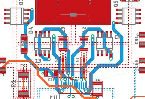
Before diving into the specifics of PCB routing, it’s essential to understand the basics. PCB routing involves creating the copper traces that connect the components on the board. The traces carry the electrical signals between the components, and their width, spacing, and length determine the signal integrity and performance of the board.
Types of PCB Routing
There are two main types of PCB routing: manual routing and autorouting.
-
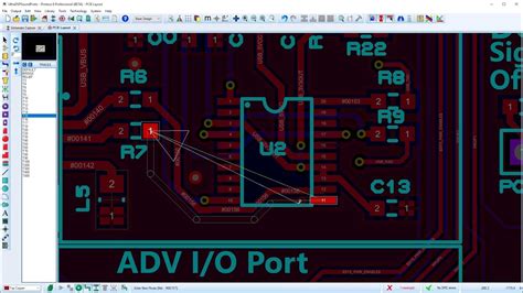
Manual routing involves manually drawing the traces on the board using PCB Design software. This method gives the designer complete control over the routing process and allows for optimization of the trace layout for better signal integrity and performance.
-
Autorouting, on the other hand, uses algorithms to automatically route the traces based on predefined rules and constraints. While autorouting can save time and effort, it may not always result in the most optimal layout, especially for complex designs.
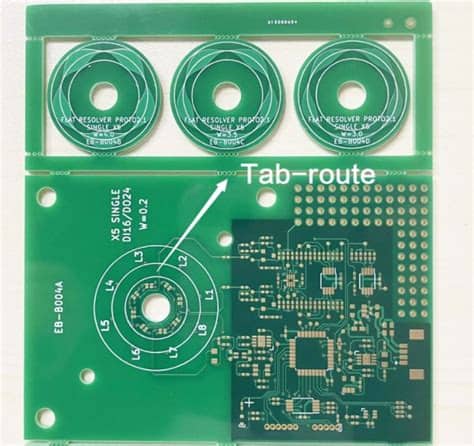
PCB Routing Layers
PCBs can have multiple layers, with each layer serving a specific purpose. The most common PCB layers are:
- Top layer: This is the top surface of the board where components are placed and routed.
- Bottom layer: This is the bottom surface of the board, which is also used for component placement and routing.
- Inner layers: These are the layers sandwiched between the top and bottom layers and are used for power and ground planes, as well as for additional routing.
The number of layers in a PCB depends on the complexity of the design and the required performance specifications.
PCB Routing Guidelines
To ensure proper PCB routing, there are several guidelines that designers should follow. These guidelines help to minimize signal interference, improve signal integrity, and ensure that the board meets the required performance specifications.
Keep Traces Short and Direct
One of the most important guidelines in PCB routing is to keep the traces as short and direct as possible. Long and meandering traces can introduce Signal Delay, increase resistance, and cause signal reflections, which can degrade the performance of the board. By keeping the traces short and direct, designers can minimize these issues and improve the overall signal integrity of the board.
Avoid Sharp Angles
Another important guideline is to avoid sharp angles in the traces. Sharp angles can cause signal reflections and create impedance mismatches, which can degrade the signal quality. Instead, designers should use smooth curves and 45-degree angles to route the traces.
Maintain Proper Trace Width and Spacing
The width and spacing of the traces are critical factors in PCB routing. The trace width determines the current-carrying capacity of the trace, while the spacing between traces determines the amount of crosstalk and signal interference. Designers should follow the manufacturer’s guidelines for trace width and spacing based on the required current and voltage levels, as well as the PCB material and thickness.
Use Ground Planes
Using ground planes is another important guideline in PCB routing. Ground planes provide a low-impedance return path for the signals and help to minimize signal interference and crosstalk. Designers should use a solid ground plane on one or more layers of the board and connect all the ground pins of the components to the ground plane using vias.
Route High-Speed Signals First
When routing a PCB, designers should start with the high-speed signals first. High-speed signals are more susceptible to signal integrity issues and require careful routing to minimize interference and maintain signal quality. By routing the high-speed signals first, designers can ensure that they have the shortest and most direct path possible, and can avoid interference from other signals.
Keep Analog and Digital Signals Separate
In mixed-signal designs that include both analog and digital circuits, it’s essential to keep the analog and digital signals separate to minimize interference. Analog signals are more sensitive to noise and interference than digital signals, and can be easily corrupted by digital noise. Designers should use separate power and ground planes for analog and digital circuits, and should route the analog and digital signals on separate layers of the board.
Use Vias Sparingly
Vias are used to connect traces between different layers of the board, but they can also introduce signal integrity issues if used excessively. Vias can cause impedance mismatches, signal reflections, and crosstalk, which can degrade the signal quality. Designers should use vias sparingly and only when necessary, and should follow the manufacturer’s guidelines for via size and spacing.
Common PCB Routing Mistakes to Avoid
In addition to following the guidelines above, designers should also be aware of common PCB routing mistakes that can lead to signal integrity issues and board failures. Some of the most common PCB routing mistakes include:
Routing Traces Too Close to the Edge of the Board
Routing traces too close to the edge of the board can cause signal integrity issues and make the board more susceptible to damage during handling and assembly. Designers should maintain a minimum clearance between the traces and the edge of the board based on the manufacturer’s guidelines.
Routing Traces Through Connector Pins
Routing traces through connector pins can cause signal integrity issues and make the board more difficult to assemble. Designers should avoid routing traces through connector pins and should instead route them around the connector or use vias to connect the traces to the connector pins.
Not Considering Thermal Management
Thermal management is an essential consideration in PCB routing, especially for high-power designs. Designers should consider the heat dissipation requirements of the components and should use thermal vias and copper pours to help dissipate heat away from the components.
Not Considering Manufacturing Constraints
Manufacturing constraints are another important consideration in PCB routing. Designers should consider the capabilities and limitations of the PCB manufacturer, including the minimum trace width and spacing, via size and spacing, and drill hole size and spacing. By considering these constraints early in the design process, designers can avoid costly redesigns and manufacturing delays.

PCB Routing Tools and Software
PCB routing can be a complex and time-consuming process, but there are many tools and software available to help designers streamline the process and ensure proper routing. Some of the most popular PCB routing tools and software include:
| Software | Description |
|---|---|
| Altium Designer | A comprehensive PCB design tool that includes advanced routing features and 3D visualization capabilities. |
| Eagle | A popular PCB design tool that includes a schematic editor, board editor, and autorouter. |
| KiCad | An open-source PCB design tool that includes a schematic editor, board editor, and autorouter. |
| OrCAD | A professional-grade PCB design tool that includes advanced routing features and simulation capabilities. |
These tools offer a range of features and capabilities, from basic schematic capture and board layout to advanced routing and simulation. Designers should choose the tool that best fits their needs and budget, and should take advantage of the training and support resources available to help them get started.
Frequently Asked Questions (FAQ)
- What is the difference between manual routing and autorouting?
-
Manual routing involves manually drawing the traces on the board using PCB design software, while autorouting uses algorithms to automatically route the traces based on predefined rules and constraints. Manual routing gives the designer complete control over the routing process, while autorouting can save time and effort but may not always result in the most optimal layout.
-
What are the most common PCB routing layers?
-
The most common PCB routing layers are the top layer, bottom layer, and inner layers. The top and bottom layers are used for component placement and routing, while the inner layers are used for power and ground planes, as well as for additional routing.
-
Why is it important to keep traces short and direct?
-
Keeping traces short and direct helps to minimize signal delay, increase resistance, and reduce signal reflections, which can degrade the performance of the board. By keeping the traces short and direct, designers can improve the overall signal integrity of the board.
-
What are the benefits of using ground planes in PCB routing?
-
Ground planes provide a low-impedance return path for the signals and help to minimize signal interference and crosstalk. By using a solid ground plane on one or more layers of the board and connecting all the ground pins of the components to the ground plane using vias, designers can improve the signal integrity of the board.
-
What are some common PCB routing mistakes to avoid?
- Some common PCB routing mistakes to avoid include routing traces too close to the edge of the board, routing traces through connector pins, not considering thermal management, and not considering manufacturing constraints. By avoiding these mistakes, designers can ensure proper routing and avoid signal integrity issues and board failures.
Conclusion
PCB routing is a critical step in the PCB design process that requires careful consideration and attention to detail. By following the guidelines and best practices outlined in this article, beginners can ensure proper routing and minimize signal integrity issues and board failures. Whether using manual routing or autorouting, designers should take advantage of the tools and resources available to streamline the process and ensure the best possible results. With practice and experience, PCB routing can become a straightforward and rewarding process that leads to high-quality, reliable PCBs.
No responses yet