Introduction to PCB Layout Design
Printed Circuit Board (PCB) layout design is a crucial step in the development of electronic devices. It involves the arrangement of components and the creation of conductive paths on a PCB to ensure proper functionality, reliability, and manufacturability of the final product. A well-designed PCB layout can minimize signal interference, reduce manufacturing costs, and improve the overall performance of the device.
The Importance of Professional PCB Layout Services
Designing a PCB layout requires expertise in various areas, including electronic design, component placement, signal integrity, and manufacturing processes. Professional PCB layout services offer the following benefits:
-
Expertise: Professional PCB Layout Designers have the knowledge and experience to create optimal layouts that meet the specific requirements of your project.
-
Time-saving: Outsourcing your PCB layout design to professionals allows you to focus on other aspects of your project while ensuring that the layout is completed efficiently.
-
Cost-effective: Professional PCB layout services can help you avoid costly mistakes and redesigns, ultimately saving you time and money.
-
Quality: Professional designers use industry-standard tools and follow best practices to ensure that your PCB layout meets the highest quality standards.
The PCB Layout Design Process
1. Schematic Review and Design
The first step in the PCB layout process is to review the schematic design. The schematic provides a graphical representation of the electronic components and their interconnections. The PCB layout designer must ensure that the schematic is accurate, complete, and follows the design requirements.
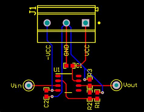
2. Component Placement
Once the schematic is finalized, the next step is to place the components on the PCB. The placement of components is critical to the overall performance and manufacturability of the PCB. Factors to consider during component placement include:
- Signal integrity: Components should be placed to minimize signal interference and ensure proper signal routing.
- Thermal management: Components that generate heat should be placed in a way that allows for proper heat dissipation.
- Manufacturing constraints: Component placement should consider the limitations of the manufacturing process, such as minimum spacing requirements and component orientation.
3. Signal Routing
After the components are placed, the next step is to route the signals between them. Signal routing involves creating conductive paths (traces) on the PCB to connect the components according to the schematic. The PCB layout designer must consider several factors during signal routing, including:
- Signal integrity: Traces should be routed to minimize crosstalk, reflections, and other signal integrity issues.
- Impedance control: Traces for high-speed signals may require impedance control to ensure proper signal propagation.
- EMI/EMC: Traces should be routed to minimize electromagnetic interference (EMI) and ensure electromagnetic compatibility (EMC).
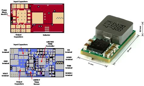
4. Power and Ground Planes
Power and ground planes are essential for providing a stable and low-impedance power supply to the components on the PCB. The PCB layout designer must create power and ground planes that are appropriate for the current requirements of the components and minimize voltage drops across the board.
5. Design Rule Check (DRC)
Before finalizing the PCB layout, the designer must perform a design rule check (DRC) to ensure that the layout meets the manufacturing constraints and design requirements. The DRC checks for issues such as minimum trace width, minimum spacing between components, and drill hole sizes.
6. Output Files Generation
Once the PCB layout is finalized and has passed the DRC, the designer generates the output files required for manufacturing. These files typically include:
- Gerber files: These files contain the information needed to manufacture the PCB, including the copper layers, solder mask, and silkscreen.
- Drill files: These files specify the location and size of the drill holes on the PCB.
- Pick and place files: These files provide the location and orientation of the components on the PCB for automated assembly.
Choosing the Right PCB Layout Design Service
When selecting a PCB layout design service, consider the following factors:
-
Experience: Choose a service provider with a proven track record of designing PCB layouts for projects similar to yours.
-
Capabilities: Ensure that the service provider has the necessary tools, expertise, and resources to handle your specific PCB layout requirements.
-
Communication: Look for a service provider that maintains clear and open communication throughout the design process to ensure that your requirements are met.
-
Turnaround time: Consider the service provider’s turnaround time and ensure that it aligns with your project timeline.
-
Cost: Evaluate the cost of the PCB layout design service in relation to the value it provides and your project budget.

PCB Layout Design Tools and Software
Professional PCB layout designers use specialized tools and software to create PCB layouts. Some of the most popular PCB layout design tools include:
| Tool | Description |
|---|---|
| Altium Designer | A comprehensive PCB design tool that offers schematic capture, 3D modeling, and advanced routing capabilities. |
| Cadence Allegro | A powerful PCB design solution that provides advanced features for high-speed design and complex layouts. |
| Mentor Graphics PADS | A suite of PCB design tools that offer schematic capture, layout, and simulation capabilities. |
| KiCad | A free and open-source PCB design tool that provides schematic capture, layout, and 3D visualization features. |
These tools offer a range of features and capabilities to streamline the PCB layout design process and ensure high-quality results.
Best Practices for PCB Layout Design
To create a successful PCB layout, consider the following best practices:
-
Keep signal paths short: Minimize the length of signal traces to reduce signal integrity issues and improve overall performance.
-
Use ground planes: Incorporate ground planes to provide a low-impedance return path for signals and minimize EMI.
-
Minimize crosstalk: Route traces to minimize crosstalk between signals, especially for high-speed designs.
-
Consider thermal management: Place components and route traces in a way that promotes proper heat dissipation and prevents thermal issues.
-
Follow manufacturing constraints: Adhere to the manufacturing constraints specified by your PCB fabrication and assembly partners to ensure a smooth and cost-effective production process.
-
Use consistent naming conventions: Establish and follow consistent naming conventions for components, nets, and other elements of the PCB layout to improve clarity and collaboration.
-
Perform thorough design reviews: Conduct regular design reviews throughout the PCB layout process to catch and address issues early on.
By following these best practices and working with experienced PCB layout design services, you can create PCB layouts that are optimized for performance, reliability, and manufacturability.
Conclusion
PCB layout design is a critical aspect of electronic product development. By working with professional PCB layout design services and following best practices, you can ensure that your PCB layout meets the specific requirements of your project while minimizing costs and time-to-market. When selecting a PCB layout design service, consider factors such as experience, capabilities, communication, turnaround time, and cost to find the best fit for your project.
Frequently Asked Questions (FAQ)
-
What is the difference between a schematic and a PCB layout?
A schematic is a graphical representation of the electronic components and their interconnections, while a PCB layout is the physical arrangement of those components and the routing of the traces on the printed circuit board. -
How long does it typically take to design a PCB layout?
The time required to design a PCB layout depends on the complexity of the design and the specific requirements of the project. Simple layouts may take a few days, while more complex layouts can take several weeks or even months. -
What are the most common PCB layout design mistakes?
Some of the most common PCB layout design mistakes include failing to consider signal integrity, neglecting thermal management, violating manufacturing constraints, and not following best practices for component placement and trace routing. -
Can I design my own PCB layout, or should I always use a professional service?
While it is possible to design your own PCB layout using specialized tools and software, it is often recommended to use a professional PCB layout design service, especially for complex or high-speed designs. Professional designers have the expertise and experience to create layouts that are optimized for performance, reliability, and manufacturability. -
How much does a professional PCB layout design service typically cost?
The cost of a professional PCB layout design service varies depending on the complexity of the design, the turnaround time, and the specific requirements of the project. Simple layouts may cost a few hundred dollars, while more complex layouts can cost several thousand dollars or more. It is essential to consider the value provided by the service and how it fits within your project budget when selecting a PCB layout design service.
No responses yet