Understanding the Role of a PCB Layout Designer
A Printed Circuit Board (PCB) Layout Designer is a crucial member of the electronic product development team. They are responsible for creating the physical layout of the PCB, which involves arranging and connecting all the electronic components according to the schematic diagram while adhering to various design rules and constraints.
The role of a PCB Layout Designer requires a unique blend of technical knowledge, attention to detail, and problem-solving skills. In this article, we will explore the key aspects of becoming a successful PCB Layout Designer.
Educational Background and Technical Skills
To become a PCB Layout Designer, a strong foundation in electronics and computer-aided design (CAD) is essential. Most employers prefer candidates with a bachelor’s degree in electrical engineering, computer engineering, or a related field. However, some designers may have an associate’s degree or a diploma in electronics coupled with relevant experience.
Key technical skills for a PCB Layout Designer include:
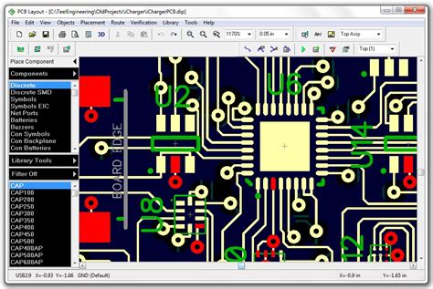
- Proficiency in PCB design software (e.g., Altium Designer, Cadence Allegro, Mentor Graphics PADS)
- Understanding of electronic components and their characteristics
- Knowledge of PCB manufacturing processes and design for manufacturability (DFM) principles
- Familiarity with industry standards and design rules (e.g., IPC, IEEE, UL)
- Understanding of signal integrity, power integrity, and electromagnetic compatibility (EMC) concepts
| Skill | Importance | Description |
|---|---|---|
| PCB Design Software | High | Proficiency in using industry-standard PCB design tools is crucial for the role. |
| Electronic Components | High | Understanding the characteristics and behavior of various electronic components. |
| DFM Principles | Medium | Knowledge of PCB manufacturing processes and designing for efficient manufacturability. |
| Industry Standards | Medium | Familiarity with relevant industry standards and design rules. |
| Signal/Power Integrity | Medium | Understanding the principles of maintaining signal and power integrity in PCB design. |
Soft Skills and Personal Attributes
In addition to technical skills, a successful PCB Layout Designer should possess certain soft skills and personal attributes:
-
Attention to Detail: PCB layout design requires meticulous attention to detail to ensure that all components are placed accurately and connected correctly.
-
Problem-Solving Skills: Designers often face challenges such as space constraints, signal integrity issues, and thermal management. Strong problem-solving skills are essential to overcome these obstacles.
-
Communication Skills: PCB Layout Designers must effectively communicate with other team members, such as electrical engineers and mechanical designers, to ensure that the layout meets all requirements and constraints.
-
Time Management: Projects often have tight deadlines, and designers must manage their time efficiently to deliver high-quality layouts within the given timeframe.
-
Adaptability: The electronics industry is constantly evolving, and PCB Layout Designers must be adaptable to new technologies, tools, and design methodologies.

The PCB Layout Design Process
The PCB layout design process typically involves the following steps:
-
Schematic Review: The designer studies the schematic diagram to understand the circuit’s functionality and the interconnections between components.
-
Component Placement: Components are placed on the PCB according to the schematic, taking into account factors such as signal flow, thermal management, and mechanical constraints.
-
Routing: The designer creates the copper traces that connect the components, following the schematic and adhering to design rules and constraints.
-
Design Rule Check (DRC): The layout is checked against a set of predefined design rules to ensure that it meets all the required specifications and constraints.
-
Manufacturing Output: The final layout is exported in a format suitable for PCB fabrication, such as Gerber files or ODB++.
Throughout the design process, the PCB Layout Designer collaborates with other team members to address any issues or changes in requirements.
Career Path and Advancement Opportunities
PCB Layout Designers can advance their careers by taking on more complex projects, mentoring junior designers, or moving into leadership roles such as senior designer or team lead. Some designers may also choose to specialize in specific areas, such as high-speed digital design, RF/microwave design, or flexible PCBs.
Continuous learning and staying updated with the latest industry trends and technologies are crucial for career growth. Designers can enhance their skills by attending workshops, conferences, and pursuing relevant certifications, such as the Certified Interconnect Designer (CID) or the Advanced Certified Interconnect Designer (CID+) offered by the IPC.
Frequently Asked Questions (FAQ)
-
What is the average salary for a PCB Layout Designer?
The salary of a PCB Layout Designer varies depending on factors such as location, experience, and industry. According to PayScale, the average annual salary for a PCB Layout Designer in the United States is approximately $65,000, with a range of $45,000 to $95,000. -
Is a degree in electrical engineering necessary to become a PCB Layout Designer?
While a degree in electrical engineering or a related field is preferred by most employers, it is not always necessary. Some designers have an associate’s degree or a diploma in electronics, coupled with relevant experience and a strong portfolio. -
What are some common challenges faced by PCB Layout Designers?
Some common challenges include working with space constraints, managing signal integrity and power integrity, ensuring proper thermal management, and meeting tight project deadlines. -
How can I keep my skills updated as a PCB Layout Designer?
To stay updated with the latest industry trends and technologies, designers can attend workshops, conferences, and webinars, pursue relevant certifications, and engage in continuous learning through online resources and communities. -
What are some important design considerations for a PCB Layout Designer?
Important design considerations include component placement, signal routing, power distribution, thermal management, electromagnetic compatibility (EMC), and design for manufacturability (DFM).
Conclusion
Becoming a successful PCB Layout Designer requires a combination of technical knowledge, soft skills, and a passion for electronic product development. By acquiring the necessary educational background, mastering industry-standard tools, and continuously updating their skills, designers can create high-quality PCB layouts that meet the ever-evolving demands of the electronics industry.
As the electronics industry continues to grow and innovate, the role of the PCB Layout Designer remains crucial in bringing new products to life. With dedication, perseverance, and a commitment to excellence, aspiring designers can build rewarding careers in this dynamic field.
No responses yet