What is PCB edge clearance and Why is it Important?
PCB edge clearance refers to the minimum distance that must be maintained between the edge of a printed circuit board (PCB) and any copper traces, pads, or vias near the edge. This design rule is critical for ensuring the mechanical and electrical integrity of the PCB during fabrication, assembly, and operation.
Proper PCB edge clearance helps prevent several issues:
-
Mechanical damage: If copper features are too close to the edge, they may be damaged or delaminated during the depaneling process or when the PCB is being handled.
-
Electrical short-circuits: Insufficient edge clearance can lead to exposed copper on the edge of the PCB, which may cause short-circuits when in contact with conductive surfaces.
-
Soldermask coverage: Adequate edge clearance allows for proper soldermask coverage, which protects the copper features from oxidation and accidental short-circuits.
-
Compliance with industry standards: Following the recommended PCB edge clearance guidelines ensures that your design complies with industry standards and can be manufactured reliably by PCB fabrication houses.
Factors Affecting PCB Edge Clearance
Several factors influence the appropriate PCB edge clearance for a given design:
PCB Thickness
The thickness of the PCB plays a significant role in determining the minimum edge clearance. Thicker PCBs generally require larger edge clearances to accommodate the depaneling process and prevent mechanical damage. The table below provides a rough guideline for minimum edge clearance based on PCB thickness:
| PCB Thickness (mm) | Minimum Edge Clearance (mm) |
|---|---|
| 0.4 – 0.8 | 0.3 |
| 0.8 – 1.6 | 0.5 |
| 1.6 – 2.4 | 0.7 |
| 2.4 – 3.2 | 1.0 |
| 3.2 – 4.0 | 1.2 |
Copper Weight
The weight of the copper foil used in the PCB also affects the required edge clearance. Heavier copper weights, such as 2 oz or 3 oz, may require larger edge clearances to ensure proper adhesion and prevent delamination. The table below shows the typical copper weights and their corresponding thicknesses:
| Copper Weight (oz) | Thickness (μm) |
|---|---|
| 0.5 | 17.5 |
| 1 | 35 |
| 2 | 70 |
| 3 | 105 |
PCB Material
The choice of PCB material can also impact the necessary edge clearance. Some materials, such as high-frequency laminates or flexible substrates, may have different mechanical properties that require specific edge clearance considerations. Always consult with your PCB manufacturer for guidance on edge clearance requirements for specialized materials.
Manufacturing Process
The PCB manufacturing process, particularly the depaneling method, can influence the required edge clearance. Common depaneling methods include:
-
V-scoring: A V-shaped groove is cut along the edge of the panel, allowing the individual PCBs to be easily snapped apart. This method typically requires a smaller edge clearance.
-
Routing: A milling tool is used to route the individual PCBs from the panel. This method requires a larger edge clearance to accommodate the router bit diameter and prevent damage to copper features.
-
Punching: A custom-shaped die is used to punch out the individual PCBs from the panel. This method requires a larger edge clearance to account for any potential misalignment or deformation during the punching process.
Consult with your PCB manufacturer to determine the appropriate edge clearance based on their specific manufacturing processes and capabilities.

Designing for Optimal PCB Edge Clearance
To ensure your PCB design has adequate edge clearance, follow these best practices:
-
Consult the manufacturer’s guidelines: Always refer to your PCB manufacturer’s design guidelines for their recommended edge clearance values based on the specific parameters of your project (PCB thickness, copper weight, material, etc.).
-
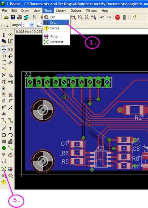
Use PCB design software: Most modern PCB design software packages include built-in design rule checks (DRCs) that can verify edge clearance and alert you to any violations. Make sure to set up the DRC rules according to your manufacturer’s guidelines.
-
Provide clear documentation: When submitting your PCB Design Files to the manufacturer, include a clear document outlining the required edge clearance and any other specific design requirements. This helps avoid misunderstandings and ensures that your design is manufactured according to your specifications.
-
Consider panelization: If your design includes multiple small PCBs, consider panelizing them into a larger array to minimize the number of edges and simplify the depaneling process. This can help reduce the impact of edge clearance requirements on your overall design.
-
Use copper pours wisely: While copper pours can be useful for shielding and thermal management, be mindful of their proximity to the PCB edges. Ensure that copper pours maintain the required edge clearance to prevent issues during manufacturing and assembly.

Common PCB Edge Clearance Pitfalls and How to Avoid Them
Despite the importance of proper PCB edge clearance, designers sometimes overlook this critical aspect or make mistakes that can lead to manufacturing issues. Here are some common pitfalls and how to avoid them:
-
Ignoring manufacturer guidelines: One of the most common mistakes is failing to consult or adhere to the PCB manufacturer’s specific edge clearance guidelines. Always make sure to obtain and follow these guidelines closely to ensure your design is manufacturable.
-
Inconsistent edge clearance: Another pitfall is having inconsistent edge clearance values throughout the PCB design. This can happen when designers manually place components and traces without properly setting up design rules in their PCB software. To avoid this, make sure to define and apply consistent edge clearance rules throughout your design.
-
Forgetting about panelization: When designing individual PCBs, it’s easy to forget that they will eventually be panelized for manufacturing. This can lead to edge clearance violations when the individual boards are combined into a panel. To prevent this, consider the panelization layout early in the design process and ensure that edge clearance is maintained both within individual boards and between adjacent boards on the panel.
-
Neglecting copper pour clearance: While copper pours are useful for shielding and thermal management, designers sometimes overlook the need for proper clearance between these pours and the PCB edge. Make sure to apply edge clearance rules to copper pours as well to avoid manufacturing issues.
-
Not considering depaneling method: Different depaneling methods (e.g., v-scoring, routing, punching) have different edge clearance requirements. Failing to consider the specific depaneling method used by your manufacturer can lead to design issues. Always communicate with your manufacturer about their preferred depaneling method and adjust your edge clearance accordingly.
By being aware of these common pitfalls and taking steps to avoid them, you can ensure that your PCB design has proper edge clearance and is ready for successful manufacturing.

Frequently Asked Questions (FAQ) about PCB Edge Clearance
-
What is the minimum PCB edge clearance required?
The minimum PCB edge clearance depends on various factors, such as PCB thickness, copper weight, material, and manufacturing process. As a general rule, the minimum edge clearance ranges from 0.3mm to 1.2mm for PCBs with thicknesses between 0.4mm and 4.0mm. However, always consult your PCB manufacturer for their specific guidelines. -
Can I use zero edge clearance for my PCB design?
While it may be tempting to use zero edge clearance to maximize the available board space, it is not recommended. Zero edge clearance can lead to mechanical damage, electrical short-circuits, and manufacturability issues. Always maintain the minimum edge clearance specified by your PCB manufacturer to ensure a reliable and manufacturable design. -
What happens if I violate the PCB edge clearance requirements?
Violating the PCB edge clearance requirements can lead to various issues during manufacturing and assembly, such as: - Mechanical damage to the PCB or components during depaneling
- Exposed copper on the PCB edge, leading to short-circuits
- Insufficient soldermask coverage, exposing copper to oxidation and potential short-circuits
-
Rejection of the PCB by the manufacturer due to non-compliance with their guidelines
-
How can I ensure my PCB design has proper edge clearance?
To ensure your PCB design has proper edge clearance: - Consult your PCB manufacturer’s design guidelines and follow their recommended edge clearance values
- Use PCB design software with built-in design rule checks (DRCs) to verify edge clearance and alert you to any violations
- Provide clear documentation to your manufacturer outlining the required edge clearance and any specific design requirements
- Consider panelization to minimize the number of edges and simplify the depaneling process
-
Use copper pours wisely and ensure they maintain the required edge clearance
-
Can I use different edge clearance values for different parts of my PCB?
In general, it is best to maintain consistent edge clearance throughout your PCB design to ensure manufacturability and avoid confusion. However, there may be cases where different edge clearance values are necessary, such as when using different PCB thicknesses or materials in the same design. In these situations, clearly communicate the specific requirements to your manufacturer and ensure that the different edge clearance zones are clearly defined in your design files.
Conclusion
PCB edge clearance is a critical design consideration that ensures the mechanical and electrical integrity of your PCB during fabrication, assembly, and operation. By understanding the factors that influence edge clearance, following best design practices, and avoiding common pitfalls, you can create reliable and manufacturable PCB designs.
Always consult with your PCB manufacturer for their specific edge clearance guidelines and requirements, as these can vary depending on the unique parameters of your project. By maintaining open communication and collaboration with your manufacturer, you can ensure that your PCB design is optimized for success.

No responses yet