Understanding the Basics of PCB Design
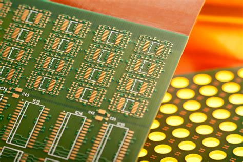
Before diving into the details of PCB design, it is essential to understand the basics. A PCB is a flat board made of insulating materials, such as fiberglass or ceramic, with conductive copper traces printed on its surface. These traces connect various electronic components, such as resistors, capacitors, and integrated circuits (ICs), to form a complete electronic circuit.
Types of PCBs
There are three main types of PCBs:
- Single-sided PCBs: These have conductive traces on only one side of the board.
- Double-sided PCBs: These have conductive traces on both sides of the board, connected through vias (small holes filled with conductive material).
- Multi-layer PCBs: These consist of multiple layers of conductive traces separated by insulating layers, allowing for more complex designs and higher component density.
PCB Design Software
To create a PCB design, you will need to use specialized software. Some popular PCB design software options include:
- Altium Designer
- KiCad
- Eagle
- OrCAD
- Cadence Allegro
These software tools provide a user-friendly interface for designing schematics, laying out components, and routing traces.
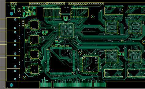
PCB Design Process
The PCB design process involves several steps, each of which requires careful consideration to ensure the best possible outcome.
Step 1: Schematic Design
The first step in PCB design is to create a schematic diagram of the electronic circuit. A schematic is a graphical representation of the components and their interconnections. It serves as a blueprint for the PCB layout.
When designing a schematic, consider the following:
- Choose the appropriate components based on their specifications and the circuit requirements.
- Use standardized symbols for components to ensure clarity and readability.
- Assign unique reference designators to each component for easy identification.
- Use net labels to identify signal paths and connections between components.
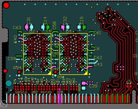
Step 2: Component Placement
Once the schematic is complete, the next step is to place the components on the PCB layout. Proper component placement is crucial for several reasons:
- It affects the overall size and shape of the PCB.
- It determines the routing of traces and the complexity of the design.
- It impacts the performance and reliability of the circuit.
When placing components, consider the following guidelines:
- Group related components together to minimize trace lengths and improve signal integrity.
- Place sensitive components, such as high-speed devices or analog circuits, away from sources of noise and interference.
- Ensure adequate spacing between components to allow for proper soldering and assembly.
- Consider the mechanical constraints of the enclosure or housing in which the PCB will be installed.
Step 3: Trace Routing
After placing the components, the next step is to route the traces that connect them. Trace routing is a critical aspect of PCB design, as it directly affects the performance and reliability of the circuit.
When routing traces, follow these guidelines:
- Use the appropriate trace width based on the current carrying capacity and the desired impedance.
- Minimize trace lengths to reduce Signal Delay and attenuation.
- Avoid sharp corners and use smooth curves to prevent signal reflections and impedance discontinuities.
- Maintain adequate spacing between traces to minimize crosstalk and interference.
- Use ground planes and power planes to provide low-impedance paths for return currents and to reduce noise.
Step 4: Design Rule Check (DRC)
After completing the trace routing, it is essential to perform a Design Rule Check (DRC). A DRC is an automated process that verifies the PCB design against a set of predefined rules and constraints. These rules ensure that the design meets the manufacturing requirements and the desired performance specifications.
Some common DRC checks include:
- Minimum trace width and spacing
- Minimum drill size and spacing
- Solder mask and silkscreen clearances
- Component footprint and pad sizes
- Copper pour and thermal relief requirements
If the DRC identifies any violations, you must modify the design to resolve them before proceeding to the next step.
Step 5: Gerber File Generation
The final step in the PCB design process is to generate Gerber files. Gerber files are industry-standard files that contain all the information needed to manufacture the PCB. They include data such as the copper layers, solder mask, silkscreen, and drill holes.
When generating Gerber files, ensure that you:
- Use the correct file format and extensions (e.g., .gbr for copper layers, .drl for drill files)
- Include all the necessary layers and files (e.g., top and bottom copper, solder mask, silkscreen)
- Specify the appropriate units and resolution (e.g., inches or millimeters, 2:4 or 2:5 precision)
- Provide a clear and concise readme file with instructions for the manufacturer
PCB Design Considerations
In addition to the basic steps of PCB design, there are several other factors to consider to ensure optimal performance and reliability.
Signal Integrity
Signal integrity refers to the quality of the signals transmitted through the PCB traces. To maintain signal integrity, consider the following:
- Use controlled impedance traces for high-speed signals to minimize reflections and distortions.
- Terminate high-speed signals with appropriate resistors to prevent ringing and overshoot.
- Use differential pairs for balanced signals to reduce electromagnetic interference (EMI).
- Minimize the use of vias, especially for high-speed signals, to reduce impedance discontinuities.
Power Integrity
Power integrity refers to the quality of the power supply distributed throughout the PCB. To ensure proper power integrity, consider the following:
- Use appropriate decoupling capacitors near power pins of ICs to reduce noise and voltage fluctuations.
- Use wide traces or copper pours for power distribution to minimize voltage drop and resistance.
- Separate analog and digital power supplies to prevent cross-contamination of noise.
- Use a star topology for power distribution to minimize ground loops and voltage gradients.
Electromagnetic Compatibility (EMC)
EMC refers to the ability of the PCB to function properly in the presence of electromagnetic interference and to minimize its own electromagnetic emissions. To improve EMC, consider the following:
- Use proper grounding techniques, such as a ground plane or grid, to provide a low-impedance path for return currents.
- Minimize the loop area of current-carrying traces to reduce magnetic field emissions.
- Use shielding techniques, such as metal enclosures or conductive coatings, to reduce radiated emissions and susceptibility.
- Follow regulatory guidelines and standards, such as FCC Part 15 or CISPR 22, for electromagnetic compatibility.
Thermal Management
Thermal management is essential to ensure that the PCB and its components operate within their specified temperature ranges. To manage heat dissipation, consider the following:
- Use appropriate copper pour and thermal vias to conduct heat away from high-power components.
- Provide adequate spacing between components to allow for air flow and convective cooling.
- Use thermal interface materials, such as thermal pads or heat sinks, to enhance heat transfer from components to the PCB or enclosure.
- Consider the use of Active Cooling methods, such as fans or thermoelectric coolers, for high-power applications.

PCB Manufacturing and Assembly
Once the PCB design is complete and the Gerber files are generated, the next step is to send the files to a PCB manufacturer for fabrication and assembly.
Choosing a PCB Manufacturer
When selecting a PCB manufacturer, consider the following factors:
- Experience and reputation in the industry
- Quality control processes and certifications (e.g., ISO 9001, UL, IPC)
- Available materials and finishes (e.g., FR-4, ENIG, HASL)
- Minimum feature sizes and tolerances
- Lead time and pricing
PCB assembly Options
There are two main options for PCB assembly:
- Through-hole assembly: Components with wire leads are inserted into holes drilled in the PCB and soldered on the opposite side.
- Surface-mount assembly: Components with flat contacts are placed on pads on the surface of the PCB and soldered in place.
Surface-mount assembly is more common in modern PCB designs due to its smaller footprint and higher component density. However, some components, such as connectors or large capacitors, may still require through-hole assembly.
PCB Inspection and Testing
After the PCB is manufactured and assembled, it is essential to perform thorough inspection and testing to ensure that it meets the design specifications and functions as intended.
Some common inspection and testing methods include:
- Visual inspection: Checking for proper component placement, soldering quality, and any visible defects.
- Automated optical inspection (AOI): Using computer vision to detect component placement and soldering defects.
- X-ray inspection: Examining the internal structure of the PCB for hidden defects, such as voids or shorts.
- In-circuit testing (ICT): Verifying the electrical connectivity and component values using a bed-of-nails test fixture.
- Functional testing: Validating the performance of the PCB under real-world operating conditions.
Frequently Asked Questions (FAQ)
-
What is the difference between a schematic and a PCB layout?
A: A schematic is a graphical representation of the electronic circuit, showing the components and their interconnections. A PCB layout is the physical arrangement of the components and traces on the printed circuit board. -
What is the purpose of a ground plane in a PCB?
A: A ground plane is a large area of copper on a PCB layer that is connected to the ground potential. It provides a low-impedance path for return currents, reduces noise and electromagnetic interference, and improves signal integrity. -
What is the difference between a via and a through-hole?
A: A via is a small hole drilled through the PCB to connect traces on different layers. It is typically filled with conductive material and does not have a component lead inserted into it. A through-hole is a larger hole drilled through the PCB to accommodate the leads of a through-hole component. -
What is the purpose of a solder mask on a PCB?
A: A solder mask is a thin, protective coating applied to the copper traces on a PCB. It serves to prevent accidental short circuits during soldering, protect the copper from oxidation and corrosion, and provide electrical insulation between adjacent traces. -
What is the difference between HASL and ENIG surface finishes?
A: HASL (Hot Air Solder Leveling) is a surface finish where the exposed copper pads are coated with a thin layer of solder using a hot air process. ENIG (Electroless Nickel Immersion Gold) is a surface finish where the copper pads are first plated with a layer of nickel, followed by a thin layer of gold. ENIG provides better flatness, solderability, and shelf life compared to HASL.
Conclusion
PCB design is a complex and iterative process that requires careful consideration of various factors, including component selection, placement, routing, signal integrity, power integrity, EMC, and thermal management. By following a well-defined PCB design guideline and using appropriate tools and techniques, you can create high-quality PCBs that meet your performance, reliability, and cost requirements.
Remember to work closely with your PCB manufacturer and assembly partner to ensure that your design is manufacturable and can be assembled efficiently. Regularly review and update your PCB design guideline based on new technologies, standards, and best practices to stay ahead of the curve in the rapidly evolving world of electronic product development.
No responses yet