What is PCB Copper Weight?
PCB copper weight refers to the thickness of the copper foil used in the manufacturing of printed circuit boards (PCBs). It is a critical factor in determining the electrical and thermal properties of the PCB, as well as its overall durability and reliability. The copper weight is typically measured in ounces per square foot (oz/ft²) or microns (µm).
Common PCB Copper Weights
| Copper Weight (oz/ft²) | Thickness (µm) |
|---|---|
| 0.5 | 17.5 |
| 1 | 35 |
| 2 | 70 |
| 3 | 105 |
| 4 | 140 |
Factors Affecting the Choice of PCB Copper Weight
When selecting the appropriate copper weight for your PCB design, consider the following factors:
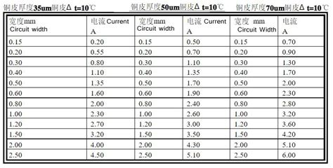
Current Carrying Capacity
The copper weight directly impacts the current carrying capacity of the PCB traces. Thicker copper foils allow for higher current flow without overheating or causing voltage drops. Use the following table as a general guide:
| Copper Weight (oz/ft²) | Current Capacity (A/mm) |
|---|---|
| 0.5 | 0.2 |
| 1 | 0.4 |
| 2 | 0.8 |
| 3 | 1.2 |
| 4 | 1.6 |
PCB Thickness and Flexibility
The overall thickness of the PCB is affected by the copper weight. Thicker copper foils result in a thicker PCB, which may be less flexible and more challenging to work with in certain applications. Consider the mechanical requirements of your project when choosing the copper weight.
Manufacturing Considerations
Different PCB manufacturers may have limitations on the copper weights they can work with. Some advanced PCB designs may require specific copper weights for fine-pitch traces or high-density interconnects. Consult with your PCB manufacturer to ensure they can accommodate your desired copper weight.
Calculating the Appropriate PCB Copper Weight
To determine the appropriate copper weight for your PCB design, follow these steps:
- Calculate the required current carrying capacity for each trace based on the components and power requirements of your circuit.
- Determine the trace width needed to support the calculated current capacity using the table provided in the “Current Carrying Capacity” section.
- Consider the overall thickness and flexibility requirements of your PCB.
- Consult with your PCB manufacturer to ensure they can accommodate your desired copper weight and trace widths.

Tips for Applying PCB Copper Weight
- Use thicker copper weights for power traces and high-current paths to minimize voltage drops and overheating.
- Consider using different copper weights for signal and power layers to optimize performance and manufacturing costs.
- Ensure proper trace spacing and isolation to prevent crosstalk and signal integrity issues, especially when using thicker copper foils.
- Work closely with your PCB manufacturer throughout the design process to ensure your copper weight choices are compatible with their capabilities and guidelines.
Frequently Asked Questions (FAQ)
1. What is the most common PCB copper weight?
The most common PCB copper weight is 1 oz/ft² (35 µm), which is suitable for a wide range of applications and is readily available from most PCB manufacturers.
2. Can I use different copper weights on the same PCB?
Yes, it is possible to use different copper weights on different layers of the same PCB. This technique is called “copper balancing” and can help optimize the electrical and thermal properties of the board while minimizing manufacturing costs.
3. What happens if I use a copper weight that is too thin?
Using a copper weight that is too thin for your application can result in insufficient current carrying capacity, leading to voltage drops, overheating, and reduced reliability of the PCB.
4. What happens if I use a copper weight that is too thick?
Using a copper weight that is too thick can increase the overall thickness and rigidity of the PCB, making it less flexible and more difficult to work with in certain applications. It can also increase manufacturing costs and lead to challenges in fine-pitch trace routing.
5. How does the copper weight affect the impedance of PCB traces?
The copper weight affects the cross-sectional area of the PCB traces, which in turn influences their impedance. Thicker copper foils result in lower Trace Impedance, while thinner copper foils lead to higher trace impedance. It is essential to consider the copper weight when designing controlled impedance traces for high-speed or RF applications.
Conclusion
PCB copper weight is a crucial factor in the design and manufacturing of printed circuit boards. By understanding the factors affecting copper weight selection and following the guidelines provided in this article, you can optimize the electrical and thermal performance of your PCB while ensuring compatibility with your manufacturing process. Remember to work closely with your PCB manufacturer and consider the specific requirements of your application when choosing the appropriate copper weight for your design.
No responses yet