Introduction to PCB Artwork
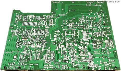
PCB artwork, also known as PCB layout or PCB Design, is the process of creating the physical representation of an electronic circuit on a printed circuit board (PCB). It involves arranging the components, routing the traces, and defining the board’s dimensions and layer stackup. Proper PCB artwork is crucial for ensuring the functionality, reliability, and manufacturability of the final product.
In this comprehensive guide, we will delve into the essential design guidelines that every PCB manufacturer should be familiar with to create high-quality and efficient PCB artwork.
The Importance of PCB Artwork Guidelines
Following well-established PCB artwork guidelines is essential for several reasons:
-
Functionality: Adhering to design guidelines helps ensure that the PCB functions as intended, with proper signal integrity, power distribution, and component placement.
-
Manufacturability: By following guidelines, PCB manufacturers can create designs that are compatible with their fabrication processes, reducing the likelihood of manufacturing defects and delays.
-
Reliability: Proper PCB artwork practices contribute to the overall reliability of the final product, minimizing the risk of failures and ensuring long-term performance.
-
Cost-effectiveness: Adhering to guidelines can help optimize the PCB design, reducing manufacturing costs and minimizing the need for expensive rework or redesigns.

Key Elements of PCB Artwork
Before diving into the specific design guidelines, let’s familiarize ourselves with the key elements of PCB artwork:
1. Component Placement
Component placement refers to the arrangement of electronic components on the PCB. Proper component placement is essential for several reasons:
- Signal integrity: Components should be placed in a way that minimizes the length of critical signal traces and reduces crosstalk and interference.
- Thermal management: Heat-generating components should be strategically placed to ensure adequate thermal dissipation and prevent overheating.
- Mechanical considerations: Component placement should account for mechanical constraints such as connectors, mounting holes, and clearances.
2. Trace Routing
Trace routing involves creating the conductive paths that connect the components on the PCB. When routing traces, consider the following factors:
- Signal integrity: Traces should be routed to minimize signal reflections, crosstalk, and electromagnetic interference (EMI).
- Impedance control: Certain traces, such as high-speed signals or differential pairs, may require specific impedance characteristics to maintain signal integrity.
- Manufacturing constraints: Trace width, spacing, and via sizes should adhere to the manufacturing capabilities of the PCB fabrication process.
3. Layer Stackup
The layer stackup defines the arrangement of conductive layers and dielectric materials in a multi-layer PCB. A well-designed layer stackup should consider:
- Signal integrity: The layer stackup should be optimized for signal integrity, with appropriate spacing between signal layers and reference planes.
- Impedance control: The dielectric materials and thicknesses should be chosen to achieve the desired impedance characteristics for controlled impedance traces.
- Manufacturability: The layer stackup should be compatible with the PCB fabrication process and adhere to the manufacturer’s capabilities and guidelines.
4. Design Rules
Design rules are a set of guidelines and constraints that ensure the manufacturability and reliability of the PCB. These rules typically include:
- Minimum trace width and spacing: The smallest allowed trace width and the minimum spacing between traces and components.
- Minimum via size and drill diameter: The smallest allowed via size and the minimum drill diameter for through-holes.
- Clearance and creepage distances: The minimum required distances between conductive elements to prevent electrical shorts and ensure insulation.

PCB Artwork Design Guidelines
Now that we understand the key elements of PCB artwork let’s explore the specific design guidelines that PCB manufacturers should follow:
1. Adhere to Industry Standards
When creating PCB artwork, it’s essential to adhere to industry standards and guidelines. Some common standards include:
- IPC standards: The IPC (Association Connecting Electronics Industries) provides a set of standards for PCB design and manufacturing, such as IPC-2221 for general design requirements and IPC-7351 for land pattern geometries.
- JEDEC standards: The JEDEC (Joint Electron Device Engineering Council) offers standards for component packaging and PCB design, such as JESD22 for reliability testing and JESD625 for pad and via dimensions.
Adhering to these standards ensures consistency, reliability, and compatibility with established manufacturing processes.
2. Follow Manufacturer’s Design Rules
Each PCB manufacturer has its own set of design rules based on their fabrication capabilities and processes. It’s crucial to obtain and follow the manufacturer’s specific design rules to ensure manufacturability and avoid potential issues. These rules may include:
- Minimum trace width and spacing
- Minimum via size and drill diameter
- Copper weight and thickness requirements
- Solder mask and silkscreen specifications
- Panelization and tooling requirements
By adhering to the manufacturer’s design rules, you can minimize the risk of manufacturing defects and delays.
3. Use a Consistent Grid System
Implementing a consistent grid system in your PCB artwork can greatly improve the organization and alignment of components and traces. A grid system helps ensure proper spacing, reduces the likelihood of design rule violations, and enhances the overall aesthetics of the PCB layout.
When choosing a grid size, consider the following factors:
- Component pitch and package dimensions
- Trace width and spacing requirements
- Via size and drill diameter
- Manufacturing capabilities and tolerances
A common grid size for surface mount components is 0.5mm or 0.025 inches, but the specific grid size may vary based on the project requirements and manufacturing constraints.
4. Optimize Component Placement
Proper component placement is crucial for achieving a well-functioning and manufacturable PCB. When placing components, consider the following guidelines:
- Group related components: Place components that are functionally related or belong to the same circuit block close together to minimize trace lengths and improve signal integrity.
- Consider component orientation: Orient components in a way that facilitates efficient routing and minimizes the number of vias required.
- Provide adequate clearances: Ensure sufficient clearance between components, traces, and board edges to accommodate manufacturing tolerances and prevent short circuits.
- Optimize for thermal management: Place heat-generating components strategically to ensure proper heat dissipation and prevent thermal issues.
- Account for mechanical constraints: Consider the placement of connectors, mounting holes, and other mechanical features to ensure compatibility with the enclosure and assembly process.
5. Route Traces Efficiently
Efficient trace routing is essential for achieving a reliable and manufacturable PCB. When routing traces, keep the following guidelines in mind:
- Minimize trace lengths: Shorter traces help reduce signal distortion, improve signal integrity, and minimize electromagnetic interference (EMI).
- Avoid sharp angles: Use 45-degree angles or curved traces instead of 90-degree angles to reduce signal reflections and improve manufacturability.
- Provide adequate trace width: Ensure that traces are wide enough to handle the required current capacity and minimize voltage drop.
- Maintain consistent trace spacing: Maintain consistent spacing between traces to minimize crosstalk and ensure manufacturability.
- Use vias strategically: Minimize the number of vias to reduce manufacturing complexity and improve signal integrity. When using vias, ensure they meet the manufacturer’s size and spacing requirements.
6. Implement Proper Grounding and Power Distribution
Proper grounding and power distribution are critical for ensuring signal integrity, reducing noise, and preventing electromagnetic interference (EMI). Consider the following guidelines:
- Use solid ground planes: Implement solid ground planes on dedicated layers to provide a low-impedance return path for signals and minimize ground bounce.
- Separate analog and digital grounds: Use separate ground planes for analog and digital circuits to prevent noise coupling and maintain signal integrity.
- Decouple power supplies: Place decoupling capacitors close to power pins of integrated circuits to minimize power supply noise and ensure stable power delivery.
- Use wide power traces: Ensure that power traces are wide enough to handle the required current capacity and minimize voltage drop.
- Implement proper power sequencing: Consider the power-up and power-down sequences of components to prevent unintended behavior and ensure reliable operation.
7. Design for Manufacturability (DFM)
Designing for manufacturability (DFM) involves creating PCB artwork that is compatible with the manufacturing processes and capabilities of the chosen PCB fabricator. DFM Guidelines help minimize manufacturing defects, improve yields, and reduce production costs.
Some key DFM considerations include:
- Adhere to minimum feature sizes: Ensure that traces, spaces, vias, and other features meet the minimum sizes specified by the manufacturer to avoid manufacturing issues.
- Provide adequate clearances: Maintain sufficient clearances between components, traces, and board edges to accommodate manufacturing tolerances and prevent short circuits.
- Use standard hole sizes: Choose standard drill sizes for through-holes and vias to minimize tooling costs and improve manufacturability.
- Avoid acute angles: Use obtuse angles or curved traces instead of acute angles to improve manufacturability and prevent acid traps during the etching process.
- Incorporate Fiducial markers: Include fiducial markers on the PCB to assist with automated assembly and ensure accurate component placement.
8. Conduct Design Reviews and Verify Manufacturability
Before finalizing the PCB artwork, it’s essential to conduct thorough design reviews and verify the manufacturability of the design. This process helps identify and address potential issues early in the design cycle, saving time and costs associated with redesigns and manufacturing delays.
Design review and verification steps may include:
- Design rule check (DRC): Perform a comprehensive design rule check to ensure that the PCB artwork adheres to the manufacturer’s design rules and constraints.
- Electrical rule check (ERC): Conduct an electrical rule check to verify the electrical connectivity and integrity of the design, including proper net assignments and power connections.
- Signal integrity analysis: Analyze critical signal paths to ensure proper signal integrity, including Impedance Matching, termination, and crosstalk reduction.
- Thermal analysis: Evaluate the thermal performance of the PCB design to ensure adequate heat dissipation and prevent thermal issues.
- Manufacturability review: Collaborate with the PCB manufacturer to review the design for manufacturability, identifying any potential issues or areas for improvement.

Best Practices for PCB Artwork Creation
In addition to following the specific design guidelines, there are several best practices that PCB manufacturers should adopt to streamline the artwork creation process and ensure high-quality results:
1. Use Appropriate Design Software
Invest in reliable and industry-standard PCB design software that offers a comprehensive set of features and tools for creating PCB artwork. Popular software options include Altium Designer, Cadence Allegro, and Mentor Graphics PADS.
When selecting design software, consider the following factors:
- Compatibility with industry standards and file formats
- Availability of component libraries and design rule checks
- Integration with simulation and analysis tools
- Ease of use and learning curve
- Scalability and performance for complex designs
- Technical support and community resources
2. Maintain Organized and Consistent Design Practices
Establish and maintain organized and consistent design practices within your PCB manufacturing team. This includes:
- Naming conventions: Use clear and consistent naming conventions for components, nets, and layers to improve readability and collaboration.
- Layer management: Assign specific purposes to each layer in the PCB Stackup and maintain a consistent layer structure across designs.
- Component libraries: Create and maintain a centralized component library with accurate footprints, 3D models, and parametric data to ensure consistency and reduce errors.
- Design templates: Develop design templates with predefined settings, layer stackups, and design rules to streamline the artwork creation process and ensure consistency across projects.
3. Collaborate and Communicate Effectively
Effective collaboration and communication among team members and stakeholders are crucial for successful PCB artwork creation. Foster a collaborative environment by:
- Design reviews: Conduct regular design reviews to gather feedback, identify potential issues, and ensure alignment with project requirements.
- Documentation: Maintain clear and comprehensive documentation, including design specifications, schematics, and bill of materials (BOM) to facilitate effective communication and knowledge sharing.
- Version control: Implement version control systems to track design changes, manage revisions, and enable easy collaboration among team members.
- Stakeholder involvement: Engage with stakeholders, including electrical engineers, mechanical designers, and manufacturing personnel, to ensure that the PCB artwork meets their requirements and constraints.
4. Continuously Improve and Adapt
The field of PCB manufacturing is constantly evolving, with advancements in materials, technologies, and design methodologies. To stay competitive and deliver high-quality PCB artwork, manufacturers must continuously improve and adapt their processes.
Some ways to foster continuous improvement include:
- Stay updated with industry trends: Keep abreast of the latest industry trends, technologies, and best practices through conferences, webinars, and industry publications.
- Invest in training and education: Provide ongoing training and education opportunities for your team members to enhance their skills and knowledge in PCB artwork creation.
- Seek feedback and learn from mistakes: Actively seek feedback from customers, suppliers, and internal stakeholders to identify areas for improvement and learn from past mistakes.
- Implement process improvements: Continuously evaluate and optimize your PCB artwork creation processes to improve efficiency, reduce errors, and enhance quality.
Frequently Asked Questions (FAQ)
1. What is the difference between PCB artwork and schematic design?
PCB artwork, also known as PCB layout, is the physical representation of the electronic circuit on the printed circuit board. It involves arranging the components, routing the traces, and defining the board’s dimensions and layer stackup. On the other hand, schematic design is the logical representation of the circuit, showing the interconnections between components using symbols and lines. The schematic captures the electrical connectivity, while the PCB artwork translates that connectivity into a physical layout.
2. Why is it important to follow the manufacturer’s design rules?
Following the manufacturer’s design rules is crucial to ensure the manufacturability and reliability of the PCB. Each manufacturer has its own set of design rules based on their fabrication capabilities and processes. These rules specify parameters such as minimum trace width and spacing, minimum via size and drill diameter, copper weight and thickness requirements, and more. Adhering to these rules minimizes the risk of manufacturing defects, improves yields, and prevents potential issues that could lead to delays or additional costs.
3. What are some common challenges in PCB artwork creation?
Some common challenges in PCB artwork creation include:
- Achieving optimal component placement while considering signal integrity, thermal management, and mechanical constraints.
- Routing complex and dense designs with high pin-count components and limited board space.
- Ensuring proper grounding and power distribution to minimize noise and electromagnetic interference.
- Adhering to the manufacturer’s design rules and constraints while meeting the project’s functional and performance requirements.
- Collaborating effectively with cross-functional teams and stakeholders to ensure alignment and timely delivery.
4. How can PCB manufacturers ensure the quality and reliability of their PCB artwork?
To ensure the quality and reliability of PCB artwork, manufacturers can follow these practices:
- Adhere to industry standards and guidelines, such as IPC and JEDEC standards, to maintain consistency and compatibility with established manufacturing processes.
- Follow the manufacturer’s specific design rules to ensure manufacturability and minimize the risk of defects.
- Conduct thorough design reviews, including design rule checks (DRC), electrical rule checks (ERC), signal integrity analysis, and thermal analysis, to identify and address potential issues early in the design cycle.
- Implement a robust quality assurance process, including visual inspections, automated optical inspection (AOI), and electrical testing, to detect and rectify any defects or anomalies.
- Foster a culture of continuous improvement by seeking feedback, learning from mistakes, and implementing process enhancements.
5. What are some best practices for managing PCB artwork revisions and changes?
Managing PCB artwork revisions and changes effectively is crucial for maintaining design integrity and ensuring smooth project execution. Some best practices include:
- Implement a version control system to track and manage design revisions, allowing for easy collaboration and rollback if needed.
- Maintain clear and comprehensive documentation, including design notes, change logs, and revision history, to facilitate effective communication and traceability.
- Establish a formal change management process that includes a review and approval workflow to ensure that all stakeholders are involved and informed of design changes.
- Perform thorough impact analysis before implementing changes to assess the potential effects on functionality, manufacturability, and project timelines.
- Communicate design changes clearly and timely to all relevant stakeholders, including manufacturing, assembly, and testing teams, to ensure smooth and synchronized execution.
Conclusion
PCB artwork creation is a critical aspect of PCB manufacturing that directly impacts the functionality, reliability, and manufacturability of the final product. By following the design guidelines outlined in this article, PCB manufacturers can ensure that their artwork meets industry standards, adheres to manufacturing constraints, and delivers high-quality results.
Remember to adhere to industry standards, follow manufacturer-specific design rules, optimize component placement and trace routing, implement proper grounding and power distribution, and design for manufacturability. Continuously review and verify your designs, collaborate effectively with stakeholders, and adopt best practices for artwork creation and revision management.
By prioritizing PCB artwork quality and continuously improving your processes, you can position your PCB manufacturing business for success in today’s competitive market. Stay updated with industry trends, invest in training and education, and foster a culture of excellence in PCB artwork creation to deliver reliable and high-performing products to your customers.

No responses yet