What is a PCB Antenna?
A PCB (Printed Circuit Board) antenna is a type of antenna that is directly integrated onto a printed circuit board. Unlike traditional antennas that are separate components connected to the PCB, a PCB antenna is a part of the PCB itself. PCB antennas are commonly used in wireless communication devices such as smartphones, tablets, laptops, and IoT (Internet of Things) devices.
PCB antennas offer several advantages over traditional antennas:
-
Space-saving: PCB antennas are compact and can be easily integrated into small devices, saving valuable space.
-
Cost-effective: Since PCB antennas are part of the PCB, they eliminate the need for additional components and manufacturing processes, reducing overall costs.
-
Improved reliability: PCB antennas are less prone to mechanical damage and connection issues compared to external antennas.
-
Design flexibility: PCB antennas can be customized to fit the specific requirements of a device, such as frequency band, gain, and radiation pattern.
Types of PCB Antennas
There are several types of PCB antennas, each with its own characteristics and applications:
Microstrip Antenna
A microstrip antenna, also known as a patch antenna, consists of a rectangular or circular metallic patch on top of a dielectric substrate, with a ground plane on the bottom. Microstrip antennas are popular for their low profile, ease of fabrication, and compatibility with PCB manufacturing processes.
Inverted-F Antenna (IFA)
An inverted-F antenna is a variant of the monopole antenna that is folded to reduce its size. It consists of a radiating element, a short-circuit plate, and a feed plate. IFAs are commonly used in mobile devices due to their compact size and omnidirectional radiation pattern.
Planar Inverted-F Antenna (PIFA)
A planar inverted-F antenna is similar to an IFA but has a planar geometry. It consists of a radiating element, a ground plane, and a shorting pin. PIFAs are often used in multi-band applications and offer good radiation efficiency and bandwidth.
Monopole Antenna
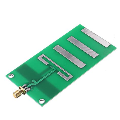
A monopole antenna is a simple and versatile antenna that consists of a single radiating element. On a PCB, a monopole antenna can be implemented as a straight or meandered trace. Monopole antennas are known for their omnidirectional radiation pattern and wide bandwidth.
Dipole Antenna
A dipole antenna consists of two symmetrical radiating elements, often implemented as two traces on a PCB. Dipole antennas offer a bidirectional radiation pattern and are commonly used in applications requiring linear polarization.

PCB Antenna Design Considerations
When designing a PCB antenna, several factors must be considered to ensure optimal performance:
-
Frequency: The antenna must be designed to operate at the desired frequency band, such as 2.4 GHz for Wi-Fi or 5 GHz for 5G networks.
-
Size and shape: The size and shape of the antenna should be optimized to fit within the available space on the PCB while meeting the performance requirements.
-
Substrate properties: The dielectric constant and thickness of the PCB substrate affect the antenna’s performance and must be considered during the design process.
-
Ground plane: The size and shape of the ground plane can significantly impact the antenna’s radiation pattern and efficiency.
-
Impedance matching: The antenna must be properly matched to the feed line to ensure maximum power transfer and minimize reflections.
-
Interference: The antenna should be designed to minimize interference from other components on the PCB and external sources.

Calculating PCB Antenna Parameters
To design a PCB antenna, several key parameters must be calculated:
Resonant Frequency
The resonant frequency (fr) of a PCB antenna is determined by its dimensions and the properties of the substrate. For a microstrip antenna, the resonant frequency can be calculated using the following equation:
fr = c / (2L√(εr))
Where:
– c is the speed of light (3 × 10⁸ m/s)
– L is the length of the radiating element
– εr is the relative permittivity of the substrate
Antenna Dimensions
The dimensions of a PCB antenna depend on the type of antenna and the desired frequency. For example, the length (L) of a microstrip antenna can be calculated using the following equation:
L = c / (2fr√(εr))
The width (W) of a microstrip antenna can be calculated using:
W = c / (2fr√((εr+1)/2))
Feed Point Location
The feed point location determines the impedance of the antenna and affects its radiation pattern. For a microstrip antenna, the feed point is typically located along the centerline of the radiating element, at a distance (d) from the edge:
d = L / (2√εr)
Bandwidth
The bandwidth of a PCB antenna is the range of frequencies over which the antenna performs satisfactorily. The bandwidth can be calculated using the following equation:
BW = (fH – fL) / fC
Where:
– fH is the upper frequency limit
– fL is the lower frequency limit
– fC is the center frequency

PCB Antenna Simulation and Optimization
To ensure optimal performance, PCB antennas are often simulated and optimized using electromagnetic simulation software, such as:
- ANSYS HFSS
- CST Studio Suite
- Altair FEKO
- Keysight ADS
These software tools allow designers to model the antenna and its surroundings, analyze its performance, and optimize its design before fabrication. Simulation results can provide valuable insights into the antenna’s radiation pattern, gain, efficiency, and other key parameters.
PCB Antenna Fabrication and Testing
Once the PCB antenna design is finalized and optimized, it can be fabricated using standard PCB manufacturing processes. The antenna is typically etched onto the PCB along with other components and traces.
After fabrication, the PCB antenna must be tested to verify its performance. Common testing methods include:
-
Return loss measurement: Measures the amount of power reflected back from the antenna due to impedance mismatch.
-
Gain measurement: Determines the antenna’s ability to concentrate radiated power in a specific direction.
-
Radiation pattern measurement: Characterizes the spatial distribution of the antenna’s radiated power.
-
Efficiency measurement: Measures the ratio of the radiated power to the input power of the antenna.
Testing results can be compared to the simulated results to validate the antenna design and identify any discrepancies or areas for improvement.
Applications of PCB Antennas
PCB antennas are widely used in various wireless communication devices and systems, such as:
- Smartphones and tablets
- Laptops and computers
- Wi-Fi routers and access points
- Bluetooth devices
- GPS receivers
- IoT sensors and devices
- Wearable devices
- Automotive systems
- Medical devices
- Industrial control systems
As wireless technologies continue to evolve and new applications emerge, the demand for compact, efficient, and cost-effective PCB antennas will continue to grow.
Challenges and Future Trends
Despite their numerous advantages, PCB antennas face several challenges:
-
Limited bandwidth: PCB antennas often have narrower bandwidths compared to traditional antennas, which can limit their application in multi-band or wideband systems.
-
Sensitivity to surroundings: PCB antennas are more susceptible to the effects of nearby components, traces, and enclosures, which can degrade their performance.
-
Complex design process: Designing and optimizing PCB antennas requires specialized knowledge and tools, which can be time-consuming and costly.
To address these challenges, researchers and engineers are exploring new materials, technologies, and design techniques for PCB antennas, such as:
-
Metamaterials: Artificial materials with unique electromagnetic properties that can enhance antenna performance and miniaturization.
-
3D printing: Additive manufacturing techniques that enable the fabrication of complex antenna structures with improved performance and flexibility.
-
Reconfigurable antennas: Antennas that can dynamically adapt their characteristics to changing operating conditions or requirements.
-
MIMO antennas: Multiple-input, multiple-output antennas that can increase data throughput and reliability in wireless communication systems.
As these technologies mature and become more accessible, PCB antennas are expected to become even more versatile, efficient, and ubiquitous in the future.
Frequently Asked Questions (FAQ)
-
What is the difference between a PCB antenna and a traditional antenna?
A PCB antenna is directly integrated onto a printed circuit board, while a traditional antenna is a separate component that is connected to the PCB. PCB antennas are more compact, cost-effective, and reliable than traditional antennas. -
What are the main types of PCB antennas?
The main types of PCB antennas include microstrip (patch) antennas, inverted-F antennas (IFA), planar inverted-F antennas (PIFA), monopole antennas, and dipole antennas. Each type has its own characteristics and applications. -
What factors should be considered when designing a PCB antenna?
When designing a PCB antenna, key factors to consider include the operating frequency, size and shape of the antenna, substrate properties, ground plane, impedance matching, and interference from other components. -
How can PCB antennas be simulated and optimized?
PCB antennas can be simulated and optimized using electromagnetic simulation software, such as ANSYS HFSS, CST Studio Suite, Altair FEKO, and Keysight ADS. These tools allow designers to model the antenna, analyze its performance, and optimize its design before fabrication. -
What are some of the challenges and future trends in PCB antenna design?
PCB antennas face challenges such as limited bandwidth, sensitivity to surroundings, and complex design processes. Future trends in PCB antenna design include the use of metamaterials, 3D printing, reconfigurable antennas, and MIMO antennas to improve performance and versatility.
No responses yet