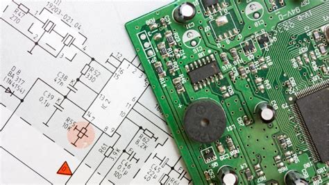
Introduction to Electromagnetic PCB routing
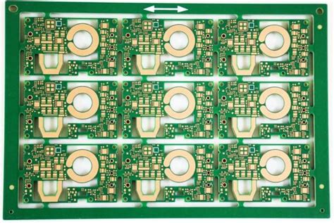
Printed Circuit Board (PCB) routing is a crucial step in the design and fabrication of electronic devices. It involves the placement and interconnection of components on a PCB while minimizing signal integrity issues, such as crosstalk, reflections, and electromagnetic interference (EMI). As the complexity and speed of electronic systems continue to increase, the need for accurate and efficient electromagnetic (EM) analysis in PCB routing becomes more critical.
Parasitic extraction is a technique used to model the unintended electrical effects that arise from the physical layout of a PCB. These effects, known as parasitics, can significantly impact the performance and reliability of the system. By accurately extracting and simulating these parasitics, designers can optimize the PCB layout to minimize their impact and ensure the proper functioning of the device.
In this article, we will explore the concepts of parasitic extraction and electromagnetic solvers in the context of PCB routing. We will discuss the various types of parasitics, their impact on signal integrity, and the methods used to extract and simulate them. Additionally, we will delve into the role of electromagnetic solvers in PCB routing and their importance in modern electronic design.
Understanding Parasitics in PCB Routing
Parasitics are the unintended electrical properties that arise from the physical layout of a PCB. These properties include resistance, capacitance, and inductance, which can affect the behavior of signals propagating through the interconnects. The three main types of parasitics in PCB routing are:
-
Resistance (R): The resistance of a conductor is determined by its material properties and geometry. It causes voltage drops and power dissipation along the interconnects, which can lead to signal attenuation and increased heat generation.
-
Capacitance (C): Capacitance occurs between adjacent conductors or between a conductor and the ground plane. It can cause signal delay, crosstalk, and power supply noise.
-
Inductance (L): Inductance is the property of a conductor that opposes changes in current flow. It can cause signal reflections, ringing, and EMI.
The impact of parasitics on signal integrity depends on various factors, such as the frequency of the signals, the length and geometry of the interconnects, and the spacing between conductors. At high frequencies, the effects of parasitics become more pronounced, leading to increased signal distortion and degradation.
To mitigate the impact of parasitics, designers must carefully consider the layout of the PCB. This involves optimizing the placement and routing of components, minimizing the length of interconnects, and using appropriate spacing and shielding techniques. However, manual optimization can be time-consuming and prone to errors, especially for complex designs. This is where parasitic extraction and electromagnetic solvers come into play.
Parasitic Extraction Techniques
Parasitic extraction is the process of identifying and modeling the parasitic elements in a PCB layout. There are several techniques used for parasitic extraction, each with its own advantages and limitations. The choice of technique depends on the complexity of the design, the desired accuracy, and the available computational resources.
1. Lumped Element Modeling
Lumped element modeling is a simplified approach to parasitic extraction, where the interconnects are represented as a network of discrete resistors, capacitors, and inductors. This method is computationally efficient and suitable for low-frequency designs or early-stage analysis. However, it may not capture the distributed nature of parasitics and can lead to inaccuracies at high frequencies.
2. Distributed Element Modeling
Distributed element modeling treats the interconnects as transmission lines with distributed resistance, capacitance, and inductance. This approach is more accurate than lumped element modeling, particularly at high frequencies, as it accounts for the spatial variation of the parasitics along the length of the interconnects. However, it requires more computational resources and may not be suitable for large-scale designs.
3. Full-Wave Electromagnetic Simulation
Full-wave electromagnetic simulation is the most accurate method for parasitic extraction, as it solves Maxwell’s equations to compute the electromagnetic fields and currents in the PCB. This approach captures the complete electromagnetic behavior of the system, including the effects of radiation, coupling, and propagation. However, full-wave simulation is computationally intensive and may require significant time and resources, especially for complex designs.
| Technique | Advantages | Limitations |
|---|---|---|
| Lumped Element Modeling | – Computationally efficient | – Limited accuracy at high frequencies |
| – Suitable for low-frequency designs | – Does not capture distributed parasitics | |
| – Fast early-stage analysis | ||
| Distributed Element Modeling | – More accurate than lumped element | – Requires more computational resources |
| – Captures distributed parasitics | – May not be suitable for large-scale designs | |
| – Suitable for high-frequency designs | ||
| Full-Wave EM Simulation | – Most accurate method | – Computationally intensive |
| – Captures complete EM behavior | – Requires significant time and resources | |
| – Accounts for radiation, coupling, etc. | – May not be feasible for complex designs |

Electromagnetic Solvers in PCB Routing
Electromagnetic solvers are computational tools that simulate the electromagnetic behavior of a PCB layout. They solve Maxwell’s equations to compute the electric and magnetic fields, currents, and voltages in the system. EM solvers are essential for accurate parasitic extraction and signal integrity analysis, particularly for high-speed and high-frequency designs.
There are several types of EM solvers used in PCB routing, each with its own strengths and weaknesses:
1. Quasi-Static Solvers
Quasi-static solvers assume that the electric and magnetic fields are decoupled and can be solved independently. They are based on the approximation that the wavelength of the signals is much larger than the dimensions of the PCB. Quasi-static solvers are computationally efficient and suitable for low-frequency designs, but they may not capture the full electromagnetic behavior at high frequencies.
2. Frequency-Domain Solvers
Frequency-domain solvers compute the electromagnetic fields and currents in the frequency domain using techniques such as the method of moments (MoM) or the finite element method (FEM). They are accurate and efficient for narrow-band simulations, where the frequency range of interest is limited. However, they may not be suitable for broadband or transient analysis.
3. Time-Domain Solvers
Time-domain solvers compute the electromagnetic fields and currents in the time domain using techniques such as the finite-difference time-domain (FDTD) method or the transmission line matrix (TLM) method. They are suitable for broadband and transient analysis, as they can capture the time-varying behavior of the system. However, they are computationally intensive and may require long simulation times.
| Solver Type | Advantages | Limitations |
|---|---|---|
| Quasi-Static Solvers | – Computationally efficient | – Limited accuracy at high frequencies |
| – Suitable for low-frequency designs | – May not capture full EM behavior | |
| Frequency-Domain Solvers | – Accurate for narrow-band simulations | – Not suitable for broadband or transient analysis |
| – Efficient for limited frequency range | ||
| Time-Domain Solvers | – Suitable for broadband and transient analysis | – Computationally intensive |
| – Captures time-varying behavior | – May require long simulation times |
The choice of EM solver depends on the specific requirements of the design, such as the frequency range of interest, the desired accuracy, and the available computational resources. In practice, a combination of different solvers may be used at different stages of the design process to balance accuracy and efficiency.

Importance of Parasitic Extraction and EM Simulation in PCB Routing
Parasitic extraction and electromagnetic simulation play a crucial role in ensuring the proper functioning and reliability of electronic systems. By accurately modeling the parasitic effects and simulating the electromagnetic behavior of the PCB, designers can:
-
Identify and mitigate signal integrity issues: Parasitic extraction and EM simulation help designers identify potential signal integrity problems, such as crosstalk, reflections, and EMI, early in the design process. This allows for timely mitigation strategies, such as optimizing the layout, using shielding techniques, or applying termination strategies.
-
Optimize the PCB layout: By iteratively extracting parasitics and simulating the electromagnetic behavior of the PCB, designers can optimize the layout to minimize the impact of parasitics and improve overall system performance. This involves techniques such as adjusting trace widths and spacings, using ground planes and power planes, and minimizing the length of critical interconnects.
-
Ensure compliance with EMC standards: Electromagnetic compatibility (EMC) standards specify the acceptable levels of electromagnetic emissions and susceptibility for electronic devices. Parasitic extraction and EM simulation help designers ensure that their PCB layouts comply with these standards by predicting and controlling the electromagnetic behavior of the system.
-
Reduce design iterations and time-to-market: By identifying and addressing signal integrity issues early in the design process, parasitic extraction and EM simulation can help reduce the number of design iterations required to achieve a functional and reliable PCB. This can significantly shorten the overall design cycle and time-to-market for electronic products.
As the complexity and speed of electronic systems continue to increase, the importance of accurate parasitic extraction and electromagnetic simulation in PCB routing becomes even more critical. With the advent of advanced packaging technologies, such as 3D integrated circuits (3D-ICs) and system-in-package (SiP), the electromagnetic interactions between components and interconnects become more complex and challenging to model. Designers must rely on state-of-the-art EM solvers and parasitic extraction tools to ensure the proper functioning and reliability of these high-density, high-speed systems.
Frequently Asked Questions (FAQ)
1. What are the main types of parasitics in PCB routing?
The three main types of parasitics in PCB routing are resistance (R), capacitance (C), and inductance (L). Resistance causes voltage drops and power dissipation along the interconnects, capacitance occurs between adjacent conductors or between a conductor and the ground plane, and inductance opposes changes in current flow.
2. What is the difference between lumped element modeling and distributed element modeling in parasitic extraction?
Lumped element modeling represents the interconnects as a network of discrete resistors, capacitors, and inductors, while distributed element modeling treats the interconnects as transmission lines with distributed resistance, capacitance, and inductance. Distributed element modeling is more accurate, particularly at high frequencies, as it accounts for the spatial variation of the parasitics along the length of the interconnects.
3. What are the advantages of full-wave electromagnetic simulation in parasitic extraction?
Full-wave electromagnetic simulation is the most accurate method for parasitic extraction, as it solves Maxwell’s equations to compute the electromagnetic fields and currents in the PCB. It captures the complete electromagnetic behavior of the system, including the effects of radiation, coupling, and propagation. However, it is computationally intensive and may require significant time and resources.
4. What are the different types of electromagnetic solvers used in PCB routing?
The three main types of electromagnetic solvers used in PCB routing are quasi-static solvers, frequency-domain solvers, and time-domain solvers. Quasi-static solvers are computationally efficient and suitable for low-frequency designs, frequency-domain solvers are accurate and efficient for narrow-band simulations, and time-domain solvers are suitable for broadband and transient analysis.
5. Why are parasitic extraction and electromagnetic simulation important in PCB routing?
Parasitic extraction and electromagnetic simulation are important in PCB routing because they help designers identify and mitigate signal integrity issues, optimize the PCB layout, ensure compliance with EMC standards, and reduce design iterations and time-to-market. As the complexity and speed of electronic systems continue to increase, accurate parasitic extraction and electromagnetic simulation become even more critical for ensuring the proper functioning and reliability of these systems.
Conclusion
Parasitic extraction and electromagnetic simulation are essential tools for designing high-performance, reliable electronic systems. By accurately modeling the parasitic effects and simulating the electromagnetic behavior of the PCB, designers can identify and mitigate signal integrity issues, optimize the layout, and ensure compliance with EMC standards. As the complexity and speed of electronic systems continue to increase, the role of advanced EM solvers and parasitic extraction techniques in PCB routing becomes even more critical.
To effectively utilize these tools, designers must have a deep understanding of the underlying concepts, such as the types of parasitics, the impact of parasitics on signal integrity, and the strengths and weaknesses of different EM solvers. They must also stay up-to-date with the latest developments in the field, such as the emergence of new modeling techniques and the integration of EM simulation with other design tools.
By leveraging the power of parasitic extraction and electromagnetic simulation, designers can create PCB layouts that are optimized for performance, reliability, and manufacturability. This, in turn, can lead to shorter design cycles, reduced costs, and improved product quality. As the electronics industry continues to push the boundaries of what is possible, the importance of these tools in PCB routing will only continue to grow.
No responses yet