What are Parasitic Capacitances?
Parasitic capacitances, also known as stray capacitances, are unintentional and unwanted capacitances that exist between conductors in electronic circuits. These capacitances arise due to the physical proximity of conductors and can have significant effects on the performance and behavior of electronic systems. In this article, we will explore the concept of parasitic capacitances, their causes, effects, and techniques to minimize their impact.
Definition and Concept
Capacitance is the ability of a system to store electrical charge. In an ideal capacitor, the capacitance is intentionally designed and controlled. However, in real-world circuits, capacitances can also exist between conductors that are not intended to form a capacitor. These unintended capacitances are called parasitic capacitances.
Parasitic capacitances occur due to the fundamental principle that whenever there are two conductors separated by an insulator (or dielectric), a capacitance exists between them. The magnitude of the parasitic capacitance depends on factors such as the surface area of the conductors, the distance between them, and the permittivity of the insulating material.
Causes of Parasitic Capacitances
Parasitic capacitances can arise from various sources in electronic circuits. Some common causes include:
-
PCB Traces: Printed circuit board (PCB) traces that run parallel to each other or in close proximity can create parasitic capacitances. The longer the traces and the closer they are to each other, the higher the parasitic capacitance.
-
Component Leads: The leads of electronic components, such as resistors, capacitors, and integrated circuits, can introduce parasitic capacitances. These capacitances exist between the leads themselves and between the leads and other conductors in the circuit.
-
Wiring and Cables: Wires and cables used to connect components in a circuit can also contribute to parasitic capacitances. The capacitance exists between the individual wires within a cable and between the cable and nearby conductors.
-
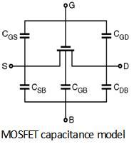
Semiconductor Junctions: In semiconductor devices, such as transistors and diodes, parasitic capacitances can occur due to the presence of PN junctions. These capacitances are known as junction capacitances and can affect the switching speed and high-frequency performance of the devices.
Effects of Parasitic Capacitances
Parasitic capacitances can have various effects on electronic circuits, depending on the specific application and the magnitude of the capacitances. Some common effects include:
Signal Distortion and Attenuation
Parasitic capacitances can cause signal distortion and attenuation, especially at high frequencies. When a signal propagates through a conductor, the parasitic capacitances along the path can act as low-pass filters, attenuating high-frequency components of the signal. This can lead to signal degradation, pulse distortion, and reduced signal integrity.
Crosstalk and Interference
Parasitic capacitances between adjacent conductors can result in crosstalk and interference. When a signal on one conductor couples to another conductor through the parasitic capacitance, it can induce unwanted voltages or currents in the neighboring conductor. This crosstalk can cause signal integrity issues, false triggering, and noise in the circuit.
Frequency Limitations
Parasitic capacitances can limit the operating frequency range of electronic circuits. At high frequencies, the reactance of the parasitic capacitances decreases, causing them to have a more significant impact on the circuit’s behavior. This can lead to reduced bandwidth, increased signal attenuation, and degraded performance.
Timing Delays
Parasitic capacitances introduce additional time constants in the circuit, which can cause timing delays. When a signal encounters a parasitic capacitance, it takes time for the capacitance to charge or discharge, resulting in a delay in the signal’s propagation. These delays can accumulate and affect the overall timing and synchronization of the system.
Power Consumption
Parasitic capacitances can contribute to increased power consumption in electronic circuits. When a signal transitions, the parasitic capacitances need to be charged and discharged, consuming additional energy. This dynamic power consumption becomes more significant at higher frequencies and can impact the power efficiency of the system.

Techniques to Minimize Parasitic Capacitances
Minimizing the impact of parasitic capacitances is crucial for optimizing the performance and reliability of electronic circuits. Several techniques can be employed to reduce the effects of parasitic capacitances:
PCB Layout Optimization
Proper PCB layout techniques can help minimize parasitic capacitances. Some guidelines include:
- Keeping high-speed signal traces as short as possible and away from other traces
- Using ground planes to shield sensitive signals
- Maintaining adequate spacing between traces and components
- Avoiding long parallel runs of traces
- Using strip line or microstrip transmission line structures for high-frequency signals
Component Selection and Placement
Careful selection and placement of components can help reduce parasitic capacitances. Some considerations include:
- Choosing components with low parasitic capacitances, such as surface-mount devices (SMDs)
- Placing components as close to each other as possible to minimize trace lengths
- Orienting components to minimize coupling between their leads
- Using shielded or coaxial cables for sensitive signals
Grounding and Shielding
Proper grounding and shielding techniques can help mitigate the effects of parasitic capacitances. Some approaches include:
- Using a solid ground plane to provide a low-impedance return path for high-frequency signals
- Implementing proper grounding strategies, such as star grounding or multi-point grounding
- Shielding sensitive signals using grounded metal enclosures or shielded cables
- Using guard rings or guard traces to isolate sensitive areas of the PCB
Simulation and Modeling
Simulation and modeling tools can be used to analyze and predict the impact of parasitic capacitances in electronic circuits. These tools allow designers to:
- Estimate the values of parasitic capacitances based on the circuit layout and component properties
- Simulate the behavior of the circuit with parasitic capacitances included
- Identify potential issues and optimize the design before physical implementation
- Perform sensitivity analysis to determine the impact of parasitic capacitances on circuit performance

Frequently Asked Questions (FAQ)
-
Q: What is the difference between parasitic capacitance and intentional capacitance?
A: Intentional capacitance is deliberately designed and controlled in a circuit to serve a specific purpose, such as filtering or energy storage. Parasitic capacitance, on the other hand, is an unintended and unwanted capacitance that arises due to the physical proximity of conductors in the circuit. -
Q: How do parasitic capacitances affect the performance of high-frequency circuits?
A: Parasitic capacitances have a more significant impact on high-frequency circuits because their reactance decreases with increasing frequency. They can cause signal attenuation, distortion, crosstalk, and timing delays, limiting the operating frequency range and degrading the overall performance of the circuit. -
Q: Can parasitic capacitances be completely eliminated in electronic circuits?
A: While it is not possible to completely eliminate parasitic capacitances, their effects can be minimized through proper circuit design, layout techniques, component selection, and shielding methods. The goal is to reduce the impact of parasitic capacitances to acceptable levels for the specific application. -
Q: How can simulation tools help in addressing parasitic capacitances?
A: Simulation tools allow designers to model and analyze the behavior of electronic circuits with parasitic capacitances included. They can estimate the values of parasitic capacitances based on the circuit layout and component properties, simulate the circuit’s performance, and identify potential issues before physical implementation. This enables designers to optimize the design and minimize the impact of parasitic capacitances. -
Q: Are there any benefits to having parasitic capacitances in electronic circuits?
A: In most cases, parasitic capacitances are undesirable and can have detrimental effects on circuit performance. However, in some specific applications, such as certain oscillator circuits or resonant networks, parasitic capacitances can be leveraged to achieve the desired functionality. Nevertheless, careful design and analysis are still required to ensure proper operation.

Conclusion
Parasitic capacitances are an inherent and often unavoidable aspect of electronic circuits. These unwanted capacitances arise due to the physical proximity of conductors and can have significant effects on signal integrity, timing, power consumption, and overall system performance. Understanding the causes and effects of parasitic capacitances is crucial for designing reliable and efficient electronic systems.
To minimize the impact of parasitic capacitances, designers can employ various techniques, including optimizing PCB layouts, selecting appropriate components, implementing proper grounding and shielding strategies, and utilizing simulation and modeling tools. By carefully considering parasitic capacitances throughout the design process, engineers can ensure the desired functionality and performance of electronic circuits.
As electronic systems continue to advance and operate at higher frequencies, the management of parasitic capacitances becomes increasingly critical. Designers must stay updated with best practices and emerging technologies to effectively address the challenges posed by parasitic capacitances and deliver robust and reliable electronic solutions.
| Component | Typical Parasitic Capacitance Range |
|---|---|
| PCB Traces | 0.1 pF – 10 pF per cm |
| Resistors (SMD) | 0.05 pF – 0.5 pF |
| Capacitors (SMD) | 0.1 pF – 1 pF |
| Integrated Circuits (SMD) | 0.1 pF – 10 pF |
| Connectors | 0.5 pF – 5 pF |
| Wires and Cables | 10 pF – 100 pF per meter |
Table 1: Typical parasitic capacitance ranges for common electronic components and structures.
The table above provides a general overview of the typical parasitic capacitance ranges associated with different electronic components and structures. These values can vary depending on factors such as the specific component package, dimensions, and dielectric materials involved. Designers can use these ranges as a starting point for estimating and considering parasitic capacitances in their circuits.
By understanding the concepts discussed in this article and applying the appropriate design techniques, engineers can effectively manage parasitic capacitances and ensure the optimal performance of their electronic systems. Embracing the challenges posed by parasitic capacitances and adopting a proactive approach to mitigate their effects will lead to more reliable, efficient, and high-performing electronic designs.
No responses yet