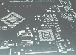
What are PCB Stencils?
PCB stencils, also known as solder paste stencils, are thin metal sheets with precisely cut openings that match the pad pattern of a printed circuit board (PCB). They are used in the solder paste application process during surface mount technology (SMT) assembly. The stencil is placed over the PCB, and solder paste is applied using a squeegee, depositing the paste through the openings onto the pads of the PCB.
PCB stencils play a crucial role in ensuring the accurate and consistent application of solder paste, which is essential for reliable solder joints and overall PCB Assembly quality. They help control the amount, placement, and uniformity of the solder paste deposited on the pads.
Types of PCB Stencils
There are several types of PCB stencils available, each with its own characteristics and advantages. The choice of stencil type depends on factors such as the complexity of the PCB design, the required precision, and the manufacturing volume. Here are the main types of PCB stencils:
1. Laser-Cut Stencils
Laser-cut stencils are made by using a high-precision laser to cut the openings in the stencil material. They offer several advantages:
- High precision and accuracy
- Smooth aperture walls for better paste release
- Suitable for fine-pitch components and complex designs
- Quick turnaround time
Laser-cut stencils are commonly made from stainless steel, which provides durability and longevity. They are a popular choice for high-volume production and demanding PCB designs.
2. Electroformed Stencils
Electroformed stencils, also known as E-FAB stencils, are created using an electrochemical process. A thin layer of nickel is deposited onto a photoresist-patterned substrate, forming the stencil with the desired openings. Electroformed stencils offer:
- Excellent dimensional accuracy and repeatability
- Smooth aperture walls for optimal paste release
- Ability to create very fine features and pitches
- Durability and long lifespan
Electroformed stencils are often used for high-precision applications, such as advanced packaging and miniaturized components.
3. Chemical Etched Stencils
Chemical etched stencils are manufactured by chemically etching the openings into a metal sheet using a photoresist mask. They have the following characteristics:
- Cost-effective for low to medium volumes
- Suitable for less complex designs and larger pitches
- Faster production compared to laser-cut or electroformed stencils
- Acceptable accuracy for most standard SMT applications
Chemical etched stencils are commonly made from stainless steel and are a good choice for prototyping or low-volume production.
Comparison Table
| Stencil Type | Precision | Complexity | Volume | Cost |
|---|---|---|---|---|
| Laser-Cut | High | High | High | High |
| Electroformed | Very High | Very High | High | High |
| Chemical Etched | Medium | Low-Medium | Low-Medium | Low-Medium |

Stencil Thickness and Aperture Design
The thickness of the PCB stencil and the design of its apertures play a critical role in the solder paste application process. The stencil thickness determines the amount of solder paste deposited on the pads, while the aperture design affects the paste release and the resulting solder joint quality.
Stencil Thickness
The choice of stencil thickness depends on several factors, including:
- Component pitch and size
- Solder paste type and viscosity
- PCB pad geometry and surface finish
- Reflow profile and process requirements
Commonly used stencil thicknesses range from 0.100 mm to 0.150 mm (4 to 6 mils) for standard SMT applications. Finer-pitch components may require thinner stencils, while thicker stencils may be used for larger components or increased solder volume.
It’s important to select the appropriate stencil thickness to ensure the right amount of solder paste is deposited on the pads. Insufficient solder paste can lead to weak solder joints or open connections, while excessive solder paste can cause bridging or tombstoning.
Aperture Design
Aperture design refers to the shape, size, and arrangement of the openings in the PCB stencil. Proper aperture design is crucial for achieving optimal solder paste release and preventing defects. Some key considerations in aperture design include:
-
Aperture size: The aperture size should be slightly larger than the PCB pad to allow for proper solder paste coverage. Typically, a 1:1 ratio between the aperture size and pad size is used as a starting point, with adjustments made based on the specific component and process requirements.
-
Aperture shape: The most common aperture shapes are square and circular. Square apertures are often used for larger pads and provide good paste release. Circular apertures are suitable for smaller pads and can help prevent bridging.
-
Aperture wall tapering: Tapering the walls of the apertures can improve solder paste release and reduce the risk of clogging. A 5-degree taper is commonly used, with the wider opening facing the PCB.
-
Area ratio: The area ratio is the ratio between the area of the aperture opening and the area of the aperture walls. A higher area ratio generally results in better paste release. An area ratio of 0.66 or higher is recommended for most applications.
Proper aperture design requires careful consideration of the PCB layout, component requirements, and manufacturing process. It often involves collaboration between the PCB designer, stencil manufacturer, and assembly team to ensure the best possible results.

Stencil Printing Process
The stencil printing process is a critical step in PCB assembly, as it directly affects the quality and reliability of the solder joints. Here’s a general overview of the stencil printing process:
-
Stencil alignment: The PCB is placed in the printer, and the stencil is aligned with the PCB using Fiducial Markers or vision systems to ensure precise registration.
-
Solder paste application: Solder paste is dispensed onto the stencil, typically using an automated dispenser or a manual squeegee.
-
Paste spreading: The squeegee is moved across the stencil, spreading the solder paste and forcing it through the apertures onto the PCB pads.
-
Stencil separation: After printing, the stencil is carefully lifted off the PCB, leaving the solder paste deposits on the pads.
-
Inspection: The printed PCB is inspected, either manually or using automated optical inspection (AOI) systems, to verify the correctness and consistency of the solder paste deposits.
Proper control of the stencil printing process parameters, such as squeegee pressure, speed, and angle, is essential for achieving high-quality solder paste deposits. Regular maintenance, including stencil cleaning and replacement, is also crucial for ensuring consistent results over time.

Costs of PCB Stencils
The cost of PCB stencils varies depending on several factors, such as the stencil type, size, thickness, and quantity. Here’s a general overview of the costs associated with different types of PCB stencils:
Laser-Cut Stencils
- Typical price range: $150 to $500 per stencil
- Higher cost compared to chemical etched stencils
- Cost-effective for high-volume production and complex designs
Electroformed Stencils
- Typical price range: $200 to $600 per stencil
- Highest cost among the three main types
- Justified for very high-precision applications and fine-pitch components
Chemical Etched Stencils
- Typical price range: $50 to $200 per stencil
- Lower cost compared to laser-cut and electroformed stencils
- Suitable for low to medium-volume production and less complex designs
It’s important to note that these are rough estimates, and actual costs may vary based on the specific requirements of the project, the stencil manufacturer, and the order quantity. In general, higher quantities lead to lower per-stencil costs due to economies of scale.
When considering the cost of PCB stencils, it’s essential to balance the upfront investment with the long-term benefits of using high-quality stencils. High-precision stencils may have a higher initial cost but can lead to better solder joint quality, reduced defects, and improved overall assembly yields, ultimately saving time and money in the manufacturing process.
Frequently Asked Questions (FAQ)
-
What is the difference between a PCB stencil and a solder paste screen?
A PCB stencil and a solder paste screen are essentially the same things. Both terms refer to the thin metal sheet with openings used to apply solder paste onto PCB pads. The term “stencil” is more commonly used in the industry. -
How often should I clean or replace my PCB stencil?
The frequency of cleaning or replacing your PCB stencil depends on factors such as the solder paste type, printing volume, and environmental conditions. As a general rule, stencils should be cleaned regularly (e.g., every 4-8 hours of printing) to prevent paste buildup and ensure consistent print quality. Stencils should be replaced when they show signs of wear, damage, or when print quality degrades. -
Can I use the same stencil for different PCB designs?
No, each PCB design requires a specific stencil that matches its unique pad layout and component requirements. Using the wrong stencil can lead to incorrect solder paste placement, insufficient or excessive solder volume, and various assembly defects. -
How do I choose the right stencil thickness for my PCB?
The choice of stencil thickness depends on factors such as the component pitch, solder paste type, and desired solder joint profile. As a general guideline, use thinner stencils (0.100-0.125 mm) for fine-pitch components and thicker stencils (0.125-0.150 mm) for larger components or increased solder volume. It’s recommended to consult with your stencil manufacturer or assembly partner to determine the optimal thickness for your specific application. -
What is the typical lifespan of a PCB stencil?
The lifespan of a PCB stencil varies depending on factors such as the stencil material, printing volume, and maintenance practices. Laser-cut and electroformed stencils generally have a longer lifespan compared to chemical etched stencils. With proper care and maintenance, a high-quality stencil can last for several thousand prints or more. However, it’s essential to regularly inspect the stencil for signs of wear or damage and replace it as necessary to maintain optimal print quality.
Conclusion
PCB stencils are an essential tool in the SMT Assembly process, enabling the precise and consistent application of solder paste onto PCB pads. By understanding the different types of stencils, their characteristics, and the key considerations in stencil design and printing, you can optimize your PCB assembly process and achieve high-quality, reliable solder joints.
When selecting a PCB stencil, consider factors such as the complexity of your PCB design, the required precision, and the production volume. Laser-cut and electroformed stencils offer the highest precision and are suitable for demanding applications, while chemical etched stencils provide a cost-effective solution for less complex designs and lower volumes.
Proper stencil thickness and aperture design are crucial for achieving the desired solder paste deposit and preventing assembly defects. Work closely with your stencil manufacturer and assembly team to determine the optimal stencil specifications for your project.
Finally, regular maintenance and inspection of your PCB stencils are essential for ensuring consistent print quality and maximizing their lifespan. By investing in high-quality stencils and following best practices in stencil printing, you can improve your PCB assembly yields, reduce defects, and ultimately save time and costs in your manufacturing process.
No responses yet