What is Over Etching in PCB Manufacturing?
Over etching is a common issue in the PCB manufacturing process where the copper traces on the printed circuit board are etched away more than intended. This can lead to several problems, such as reduced trace width, increased resistance, and potential open circuits. Over etching occurs when the etching process is not properly controlled, resulting in the removal of too much copper from the PCB.
Causes of Over Etching
There are several factors that can contribute to over etching in PCB manufacturing:
-
Incorrect Etching Time: If the PCB is left in the etching solution for too long, it can result in over etching. The etching time must be carefully controlled to ensure that the correct amount of copper is removed.
-
Incorrect Etching Solution Concentration: The concentration of the etching solution plays a crucial role in the etching process. If the solution is too strong, it can lead to over etching, while a weak solution may result in under etching.
-
Incorrect Temperature: The temperature of the etching solution can also affect the etching process. If the temperature is too high, it can accelerate the etching process, leading to over etching.
-
Uneven Etching: If the etching process is not uniform across the PCB, it can result in some areas being over etched while others are under etched. This can be caused by poor circulation of the etching solution or uneven distribution of the copper on the PCB.
Effects of Over Etching
Over etching can have several negative effects on the performance and reliability of the PCB:
-
Reduced Trace Width: Over etching can cause the copper traces to become thinner than intended, which can increase their resistance and affect the electrical performance of the PCB.
-
Increased Resistance: As the trace width decreases, the resistance of the copper traces increases. This can lead to voltage drops and Signal Integrity issues, especially in high-speed circuits.
-
Open Circuits: In severe cases of over etching, the copper traces can be completely removed, resulting in open circuits. This can render the PCB unusable and require costly rework or replacement.
-
Reduced Manufacturing Yield: Over etching can lead to a higher number of defective PCBs, reducing the overall manufacturing yield and increasing production costs.
How to Prevent Over Etching in PCB Manufacturing
Preventing over etching requires careful control and monitoring of the etching process. Here are some steps that can be taken to minimize the risk of over etching:
-
Proper Etching Time Control: The etching time must be carefully controlled to ensure that the correct amount of copper is removed. This can be achieved through the use of automated etching equipment with precise timing control.
-
Accurate Etching Solution Concentration: The concentration of the etching solution must be regularly monitored and adjusted to maintain the correct level. This can be done through the use of titration or conductivity measurements.
-
Temperature Control: The temperature of the etching solution must be maintained within a specific range to ensure consistent etching results. This can be achieved through the use of temperature-controlled etching tanks.
-
Uniform Etching: To ensure uniform etching across the PCB, the etching solution must be properly circulated and the PCB must be agitated during the etching process. This can be done through the use of spray etching or bubble etching techniques.
-
Regular Maintenance: Regular maintenance of the etching equipment and solutions is essential to ensure consistent and reliable etching results. This includes cleaning the etching tanks, replacing the etching solution when necessary, and calibrating the equipment.
Etching Methods and Their Impact on Over Etching
There are several etching methods used in PCB manufacturing, each with its own advantages and disadvantages in terms of over etching:
-
Wet Etching: Wet etching is the most common method used in PCB manufacturing. It involves immersing the PCB in an etching solution, such as ferric chloride or cupric chloride. While wet etching is relatively simple and cost-effective, it can be prone to over etching if not properly controlled.
-
Dry Etching: Dry etching uses plasma to remove the copper from the PCB. This method is more precise and can achieve finer features than wet etching. However, it is more expensive and requires specialized equipment.
-
Laser Etching: Laser etching uses a high-powered laser to remove the copper from the PCB. This method is highly precise and can achieve very fine features, but it is also the most expensive and slowest of the etching methods.
| Etching Method | Advantages | Disadvantages |
|---|---|---|
| Wet Etching | – Simple and cost-effective | – Prone to over etching |
| – High throughput | – Less precise than other methods | |
| Dry Etching | – More precise than wet etching | – More expensive |
| – Can achieve finer features | – Requires specialized equipment | |
| Laser Etching | – Highly precise | – Most expensive |
| – Can achieve very fine features | – Slowest method |
Detecting and Measuring Over Etching
Detecting and measuring over etching is essential for quality control in PCB manufacturing. There are several methods that can be used to assess the extent of over etching:
-
Visual Inspection: Over etched PCBs can often be identified through visual inspection. Signs of over etching include thin or broken traces, excessive copper removal, and uneven etching.
-
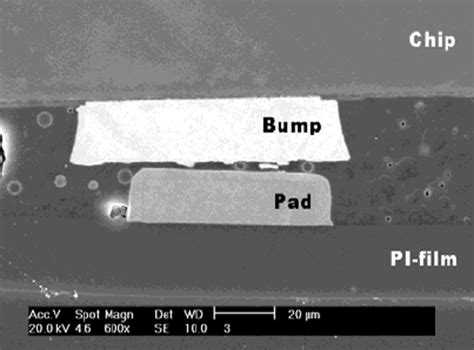
Microscopic Inspection: For more detailed analysis, microscopic inspection can be used to measure the width of the copper traces and compare them to the design specifications. This can be done using an optical microscope or a scanning electron microscope (SEM).
-
Electrical Testing: Over etching can affect the electrical performance of the PCB, such as increased resistance or open circuits. Electrical testing can be used to detect these issues and assess the extent of over etching.
-
Cross-Sectional Analysis: In some cases, cross-sectional analysis may be necessary to accurately measure the extent of over etching. This involves cutting the PCB and examining the cross-section under a microscope to measure the trace width and thickness.
Correcting Over Etched PCBs
Once over etching has been detected, there are several methods that can be used to correct the issue, depending on the severity of the over etching:
-
Copper Plating: For minor over etching, copper plating can be used to build up the thickness of the copper traces. This involves electroplating additional copper onto the existing traces to increase their width and thickness.
-
Jumper Wires: For more severe cases of over etching, jumper wires can be used to bridge the gaps in the copper traces. This involves soldering small wires between the affected traces to restore electrical continuity.
-
Rework: In some cases, the over etched PCB may need to be partially or completely reworked. This involves removing the damaged traces and replacing them with new copper traces.
-
Scrapping: If the over etching is too severe or the PCB cannot be corrected, it may need to be scrapped and replaced with a new one.

FAQ
-
What is the most common cause of over etching in PCB manufacturing?
The most common cause of over etching is incorrect etching time control. If the PCB is left in the etching solution for too long, it can result in excessive copper removal and over etching. -
How can over etching affect the performance of a PCB?
Over etching can lead to reduced trace width, increased resistance, and potential open circuits. This can affect the electrical performance of the PCB, leading to signal integrity issues and reduced reliability. -
What is the most precise etching method for preventing over etching?
Laser etching is the most precise etching method for preventing over etching. It uses a high-powered laser to remove the copper from the PCB, achieving very fine features and minimal risk of over etching. -
How can over etching be detected in PCB manufacturing?
Over etching can be detected through visual inspection, microscopic inspection, electrical testing, and cross-sectional analysis. These methods can identify signs of over etching, such as thin or broken traces, excessive copper removal, and increased resistance. -
What are the options for correcting an over etched PCB?
The options for correcting an over etched PCB depend on the severity of the over etching. Minor over etching can be corrected through copper plating, while more severe cases may require jumper wires or partial rework. In some cases, the PCB may need to be scrapped and replaced.
No responses yet