Introduction to PCB Noise Reduction
Noise reduction is a crucial aspect of designing and manufacturing printed circuit boards (PCBs) that utilize operational amplifiers (op amps). Op amps are sensitive to various types of noise, including electromagnetic interference (EMI), crosstalk, and power supply noise. Proper PCB layout techniques can significantly reduce noise and improve the overall performance of your op amp circuits.
In this comprehensive article, we will explore the best practices and guidelines for op amp layout to minimize noise in your PCB designs. By following these techniques, you can ensure that your op amp circuits operate with optimal signal integrity and reliability.
Understanding Noise Sources in Op Amp Circuits
Before diving into the layout guidelines, it’s essential to understand the common noise sources that can affect op amp circuits on a PCB. The primary noise sources include:
- Power supply noise
- Electromagnetic interference (EMI)
- Crosstalk
- Ground loops
- Thermal noise
Power Supply Noise
Power supply noise refers to the fluctuations or ripples in the voltage supplied to the op amp. These fluctuations can be caused by various factors, such as:
- Poor power supply regulation
- Inadequate decoupling capacitors
- High-frequency switching noise from nearby circuits
To minimize power supply noise, it’s crucial to use a clean and well-regulated power source, along with proper decoupling techniques, which we will discuss in detail later.
Electromagnetic Interference (EMI)
EMI is the unwanted coupling of electromagnetic energy from one circuit to another. It can be caused by various sources, including:
- High-frequency digital signals
- Switching power supplies
- External sources like radio transmitters
EMI can induce noise in sensitive analog circuits, such as op amps, leading to signal degradation and performance issues.
Crosstalk
Crosstalk occurs when signals from one circuit inadvertently couple with adjacent circuits on the PCB. This coupling can happen through:
- Capacitive coupling between traces
- Inductive coupling between loops or traces
- Shared impedance in ground or power planes
Crosstalk can introduce unwanted noise and interference in op amp circuits, affecting their accuracy and performance.
Ground Loops
Ground loops occur when there are multiple paths for ground currents to flow between different sections of a PCB. These loops can act as antennas, picking up noise and introducing it into the circuit. Ground loops can be caused by:
- Improper grounding techniques
- Incorrect use of ground planes
- Mixing analog and digital grounds
Eliminating ground loops is essential for noise reduction in op amp circuits.
Thermal Noise
Thermal noise is the random fluctuation of electrons due to the thermal energy present in all conductors. While thermal noise is inherent in all electronic components, it can be minimized by:
- Using low-noise op amps
- Proper component selection
- Optimizing circuit design
PCB layout guidelines for Noise Reduction
Now that we have a better understanding of the noise sources affecting op amp circuits let’s explore the key PCB layout guidelines for noise reduction.
1. Component Placement
Proper component placement is crucial for minimizing noise in op amp circuits. Follow these guidelines:
- Place the op amp as close as possible to its associated components, such as feedback resistors and capacitors.
- Keep the op amp away from high-frequency digital circuits, switching power supplies, and other potential noise sources.
- If using multiple op amps, separate them to minimize crosstalk and thermal interactions.
2. Power Supply Decoupling
Effective power supply decoupling is essential for reducing power supply noise in op amp circuits. Use the following techniques:
- Place decoupling capacitors as close as possible to the op amp’s power supply pins.
- Use a combination of bulk and ceramic capacitors for optimal decoupling performance.
- Consider using ferrite beads or inductors in series with the power supply to filter high-frequency noise.
| Capacitor Type | Value Range | Placement | Purpose |
|---|---|---|---|
| Bulk (e.g., tantalum, electrolytic) | 1 µF to 10 µF | Near power entry point | Low-frequency decoupling |
| Ceramic | 0.01 µF to 0.1 µF | Close to op amp power pins | High-frequency decoupling |
3. Grounding Techniques
Proper grounding is critical for minimizing ground loops and reducing noise in op amp circuits. Follow these guidelines:
- Use a solid ground plane on a dedicated PCB layer.
- Separate analog and digital grounds, connecting them at a single point, usually near the power supply.
- Use star grounding technique, where each ground connection is routed directly to the central ground point.
- Avoid splitting the ground plane or creating narrow ground paths, as this can increase impedance and introduce noise.
4. Signal Routing
Careful signal routing is essential for minimizing crosstalk and EMI in op amp circuits. Use these techniques:
- Keep sensitive analog traces away from high-frequency digital traces and power supply lines.
- Use short and direct traces for critical signals, such as the op amp’s inputs and outputs.
- Avoid running sensitive traces parallel to each other for long distances to minimize capacitive coupling.
- If crossing signal traces is necessary, do so at right angles to minimize inductive coupling.
5. Shielding
Shielding can be an effective way to reduce EMI in op amp circuits. Consider the following:
- Use shielded cables or traces for sensitive signals, especially those coming from off-board sources.
- Place sensitive op amp circuits inside a Faraday cage or shielded enclosure to minimize external EMI.
- Use guard rings or traces around sensitive analog circuits to divert unwanted signals away from the op amp.
6. Layering and Stackup
A well-designed PCB layer stackup can help reduce noise and improve signal integrity in op amp circuits. Follow these guidelines:
- Use a multi-layer PCB with dedicated layers for power, ground, and signals.
- Place the power and ground planes on adjacent layers to create a low-impedance supply path and minimize EMI.
- Use inner layers for sensitive analog signals, sandwiched between power and ground planes for shielding.
| Layer | Purpose |
|---|---|
| Top | Components, high-speed digital signals |
| Inner 1 | Ground plane |
| Inner 2 | Sensitive analog signals |
| Inner 3 | Power plane |
| Bottom | Components, low-speed signals |

Testing and Verification
After implementing the PCB layout guidelines for noise reduction, it’s essential to test and verify the performance of your op amp circuits. Use the following techniques:
-
Visual inspection: Carefully inspect the PCB for any layout errors, such as incorrect component placement or signal routing.
-
Continuity testing: Use a multimeter to ensure proper continuity between components and check for any short circuits.
-
Power supply testing: Measure the power supply voltage at the op amp pins to verify that it is within the specified range and free from excessive noise.
-
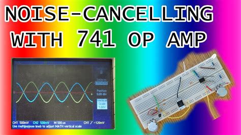
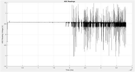
Signal integrity testing: Use an oscilloscope to measure the op amp’s input and output signals, checking for any signs of distortion, ringing, or noise.
-
EMI testing: If necessary, perform EMI testing in a specialized lab to ensure that your op amp circuit meets the required electromagnetic compatibility (EMC) standards.
Conclusion
Designing a low-noise PCB for op amp circuits requires careful consideration of various factors, including component placement, power supply decoupling, grounding, signal routing, shielding, and PCB layering. By following the guidelines outlined in this article, you can significantly reduce noise and improve the performance of your op amp circuits.
Remember that noise reduction is an iterative process, and it may take some trial and error to achieve the desired results. Always test and verify your PCB design to ensure that it meets the required specifications and performance criteria.
Frequently Asked Questions (FAQ)
-
Q: What is the most important factor in reducing noise in op amp circuits?
A: Proper grounding techniques, including the use of a solid ground plane and separating analog and digital grounds, are arguably the most critical factors in reducing noise in op amp circuits. -
Q: Can I use a single decoupling capacitor for my op amp?
A: While a single decoupling capacitor can help, it’s generally recommended to use a combination of bulk and ceramic capacitors for optimal decoupling performance across a wide frequency range. -
Q: Is it necessary to use a multi-layer PCB for op amp circuits?
A: While a multi-layer PCB is not always necessary, it can significantly improve noise reduction and signal integrity in op amp circuits by providing dedicated layers for power, ground, and sensitive signals. -
Q: How far should I keep sensitive analog traces from high-frequency digital traces?
A: As a general rule, try to keep sensitive analog traces at least 3-5 times the trace width away from high-frequency digital traces to minimize crosstalk and EMI. -
Q: Can I use a ground pour instead of a solid ground plane?
A: While a ground pour can be effective in some cases, a solid ground plane is generally preferred for op amp circuits, as it provides a lower-impedance path for return currents and helps minimize ground loops and noise.
No responses yet