Importance of Proper PCB Layout
Proper PCB layout is essential for switching power supplies and regulators due to the following reasons:
- Minimizing EMI: Switching regulators generate high-frequency noise that can interfere with sensitive analog and digital circuits on the same board or in nearby systems.
- Reducing power losses: Improper layout can lead to increased trace resistance and inductance, resulting in higher power losses and reduced efficiency.
- Improving thermal management: Optimal component placement and proper copper pour can help dissipate heat effectively, preventing thermal stress on components and improving overall system reliability.
- Enhancing system stability: A well-designed layout minimizes parasitic inductance and capacitance, which can cause ringing, oscillations, and instability in the power supply.
Key Components and Their Placement
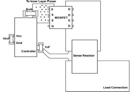
When laying out a PCB for switching power supplies and regulators, it is essential to identify the key components and place them strategically to minimize the loop area and reduce EMI. The main components include:
- Switching controller or regulator IC
- Input and output capacitors
- Inductor
- Power MOSFETs or transistors
- Rectifier diodes
- Feedback resistors and compensation components
Switching Controller or Regulator IC
The switching controller or regulator IC should be placed as close as possible to the power stage components (MOSFETs, inductor, and capacitors) to minimize trace lengths and reduce parasitic inductance. This placement also helps to keep the sensitive analog and feedback traces away from the high-current switching paths.
Input and Output Capacitors
Input and output capacitors should be placed as close as possible to the power stage components to minimize the loop area and reduce the effects of parasitic inductance. When using multiple capacitors in parallel, ensure that they are of the same type and value to promote even current sharing.
Inductor
The inductor should be placed close to the switching MOSFETs and the output capacitor to minimize trace lengths and reduce copper losses. Orient the inductor to minimize coupling with other sensitive components and traces.
Power MOSFETs or Transistors
Power MOSFETs or transistors should be placed close to the switching controller or regulator IC and the inductor to minimize the high-current loop area. Ensure that the MOSFET gate traces are as short as possible and kept away from the drain and source traces to prevent gate ringing and oscillations.
Rectifier Diodes
Rectifier diodes should be placed close to the inductor and output capacitor to minimize trace lengths and reduce losses. When using high-current diodes, consider using multiple diodes in parallel to spread the current and improve thermal performance.
Feedback Resistors and Compensation Components
Feedback resistors and compensation components should be placed close to the switching controller or regulator IC to minimize trace lengths and reduce noise pickup. Use surface-mount components whenever possible to reduce parasitic effects and improve system stability.

Grounding and Power Planes
Proper grounding and the use of power planes are essential for minimizing EMI and ensuring stable operation of switching power supplies and regulators.
Ground Planes
Use a solid ground plane on one or more layers of the PCB to provide a low-impedance return path for high-frequency currents. Connect the ground pins of the switching controller or regulator IC, MOSFETs, and other power stage components directly to the ground plane using short, wide traces or vias.
Power Planes
Use power planes for the input and output voltages to reduce trace inductance and resistance. Place the power planes on separate layers from the ground plane to minimize capacitive coupling and reduce EMI.
Star Grounding
Implement a star grounding scheme, where all ground connections for the power stage components meet at a single point, usually near the input or output capacitor. This approach helps to minimize ground loops and reduce noise coupling between different sections of the PCB.
Analog and Digital Ground Separation
Separate the analog and digital ground planes to prevent noise from the digital circuitry from interfering with sensitive analog signals. Connect the analog and digital ground planes at a single point, preferably near the power supply or regulator ground pin.

Trace Width and Routing
Proper trace width and routing techniques are crucial for minimizing losses, reducing EMI, and ensuring reliable operation of switching power supplies and regulators.
High-Current Traces
Use wide traces for high-current paths, such as the connections between the input capacitor, MOSFETs, inductor, and output capacitor. The trace width should be sufficient to handle the expected current without causing excessive temperature rise or voltage drop.
Trace Length Minimization
Minimize the length of high-current traces to reduce parasitic inductance and resistance. Keep the traces as short and direct as possible, avoiding unnecessary bends or meandering paths.
Trace Spacing
Maintain adequate spacing between high-current traces and sensitive analog or digital traces to minimize crosstalk and noise coupling. Use ground traces or planes to provide shielding between sensitive traces and high-current paths.
Kelvin Connections
Use Kelvin connections for sensitive nodes, such as the feedback resistors and the current sense resistor. A Kelvin connection is a four-terminal connection that separates the high-current path from the sensing path, minimizing the impact of trace resistance on the measurement accuracy.
EMI Reduction Techniques
In addition to the layout techniques mentioned above, several other methods can be employed to reduce EMI in switching power supplies and regulators.
Snubber Circuits
Use snubber circuits, consisting of a resistor and a capacitor in series, across the switching MOSFETs to suppress voltage spikes and ringing caused by the parasitic inductance in the circuit. Properly designed snubber circuits can significantly reduce EMI and improve system stability.
Ferrite Beads
Place ferrite beads on the input and output power lines to suppress high-frequency noise. Ferrite beads act as high-impedance elements at high frequencies, attenuating noise without significantly affecting the DC voltage.
Shielding
Use shielding techniques, such as metal cans or shields, to contain EMI generated by the switching power supply or regulator. Shielding can be particularly effective in preventing radiated EMI from coupling into nearby sensitive circuits.
Spread-Spectrum Techniques
Implement spread-spectrum techniques, where the switching frequency is modulated over a range of frequencies, to reduce the peak EMI levels. This approach spreads the energy of the switching noise over a wider frequency range, making it easier to comply with EMI regulations.
Thermal Management
Proper thermal management is essential for ensuring the reliable operation of switching power supplies and regulators. The following techniques can be used to improve thermal performance:
Copper Pour
Use copper pour on the PCB layers to create a thermal mass that helps to spread heat and reduce component temperatures. Copper pour can be particularly effective when used in conjunction with thermal vias to transfer heat to other layers of the PCB.
Thermal Vias
Place thermal vias beneath power dissipating components, such as MOSFETs and rectifier diodes, to transfer heat to the other layers of the PCB and the ground plane. Thermal vias help to reduce component temperatures and improve overall system reliability.
Heatsinks
Use heatsinks on power dissipating components to increase the surface area for heat dissipation and lower component temperatures. Heatsinks can be attached to the components using thermal adhesive or mechanical fasteners, depending on the specific requirements of the application.
Component Placement
Place power dissipating components away from heat-sensitive components, such as the switching controller or regulator IC, to minimize thermal interaction and ensure reliable operation.
PCB Layer Stackup
The PCB layer stackup plays a crucial role in determining the performance and EMI characteristics of switching power supplies and regulators. Consider the following guidelines when designing the layer stackup:
Layer Count
Use a sufficient number of layers to accommodate the necessary power planes, ground planes, and signal routing. A typical layer stackup for a switching power supply or regulator may consist of four or more layers.
Layer Arrangement
Arrange the layers to minimize the loop area and provide effective shielding between sensitive traces and high-current paths. A common arrangement is to have the power planes on the inner layers, with the ground planes on the outer layers to provide shielding.
Dielectric Thickness
Choose the appropriate dielectric thickness between layers to achieve the desired impedance and minimize capacitive coupling. Thinner dielectrics can help to reduce the loop area and improve system performance, but may also increase the manufacturing complexity and cost.
Testing and Verification
After completing the PCB layout, it is essential to perform thorough testing and verification to ensure that the switching power supply or regulator meets the desired performance and EMI requirements.
Functional Testing
Perform functional testing to verify that the power supply or regulator operates as expected under various load conditions and input voltage ranges. Measure the output voltage, ripple, and transient response to ensure compliance with the specifications.
EMI Testing
Conduct EMI testing to measure the conducted and radiated emissions from the switching power supply or regulator. Ensure that the emissions levels comply with the relevant EMI standards and regulations, such as CISPR, FCC, or EN standards.
Thermal Testing
Perform thermal testing to verify that the components operate within their specified temperature ranges under worst-case load and ambient temperature conditions. Use thermal imaging cameras or thermocouples to measure the temperature of critical components and ensure that the thermal management techniques are effective.
Frequently Asked Questions (FAQ)
- Q: What is the importance of minimizing loop area in switching power supply and regulator layouts?
A: Minimizing the loop area in switching power supply and regulator layouts is crucial for reducing parasitic inductance and minimizing EMI. By keeping the high-current paths as short and direct as possible, the layout minimizes the generation of unwanted magnetic fields and helps to improve system stability and performance.
- Q: How can I reduce EMI in my switching power supply or regulator design?
A: There are several techniques to reduce EMI in switching power supply and regulator designs, including:
– Minimizing loop areas and trace lengths
– Using snubber circuits to suppress voltage spikes and ringing
– Implementing spread-spectrum techniques to reduce peak EMI levels
– Using ferrite beads and shielding to suppress high-frequency noise
– Properly grounding and using power planes to provide low-impedance return paths
- Q: What are the benefits of using a star grounding scheme in switching power supply and regulator layouts?
A: A star grounding scheme, where all ground connections for the power stage components meet at a single point, helps to minimize ground loops and reduce noise coupling between different sections of the PCB. By providing a single, low-impedance path for ground currents, star grounding improves system stability and helps to minimize EMI.
- Q: How can I ensure proper thermal management in my switching power supply or regulator layout?
A: Proper thermal management in switching power supply and regulator layouts can be achieved through several techniques, such as:
– Using copper pour to create a thermal mass and spread heat
– Placing thermal vias beneath power dissipating components to transfer heat to other layers
– Using heatsinks to increase the surface area for heat dissipation
– Strategically placing power dissipating components away from heat-sensitive components
- Q: What should I consider when designing the PCB layer stackup for a switching power supply or regulator?
A: When designing the PCB layer stackup for a switching power supply or regulator, consider the following:
– Use a sufficient number of layers to accommodate power planes, ground planes, and signal routing
– Arrange the layers to minimize loop area and provide effective shielding
– Choose the appropriate dielectric thickness to achieve the desired impedance and minimize capacitive coupling
– Place power planes on inner layers and ground planes on outer layers for effective shielding
By following these PCB layout guidelines and best practices, designers can create robust, efficient, and EMI-compliant switching power supplies and regulators. Proper layout techniques, combined with careful component selection and thorough testing, will ensure optimal system performance and reliability.
No responses yet