What is ODB++?
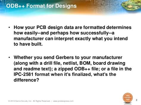
ODB++ is a comprehensive and intelligent data exchange format that encapsulates all the necessary information required for PCB fabrication. It is a single file database that includes both the PCB design data and the manufacturing information, ensuring that the design intent is accurately conveyed to the fabrication process.
The ODB++ format is designed to be independent of any specific CAD or CAM system, allowing for easy data exchange between different tools and vendors. It supports a wide range of PCB Technologies, including rigid, flex, and Rigid-Flex Designs, as well as advanced features such as embedded components and high-density interconnects (HDI).
Benefits of Using ODB++
Using ODB++ as the data exchange format for PCB fabrication offers several advantages:
-
Completeness: ODB++ includes all the necessary information for PCB fabrication in a single file, eliminating the need for multiple files and reducing the risk of errors or omissions.
-
Accuracy: The intelligent data structure of ODB++ ensures that the design intent is accurately captured and conveyed to the manufacturing process, minimizing the chances of misinterpretation or ambiguity.
-
Efficiency: By providing a standardized format for data exchange, ODB++ streamlines the communication between PCB designers and manufacturers, reducing the time and effort required for data preparation and translation.
-
Flexibility: ODB++ supports a wide range of PCB technologies and features, making it suitable for various applications and industries.
-
Collaboration: The ODB++ format facilitates collaboration between different teams and organizations involved in the PCB design and fabrication process, as it provides a common language for data exchange.

ODB++ File Structure
The ODB++ file structure is organized in a hierarchical manner, with different directories and files representing various aspects of the PCB design and manufacturing data. Here is an overview of the main components of an ODB++ file:
| Directory/File | Description |
|---|---|
matrix/matrix |
Contains the board outline, layer stackup, and other general information about the PCB. |
steps/pcb/layers |
Contains the layer-specific data, such as copper features, soldermask, and silkscreen. |
steps/pcb/components |
Contains the component placement data, including reference designators and locations. |
steps/pcb/artwork |
Contains the artwork files for the PCB, such as logos or custom graphics. |
steps/pcb/drill |
Contains the drilling data, including drill sizes and locations. |
steps/pcb/netlist |
Contains the netlist information, describing the connectivity between components. |
steps/pcb/eda |
Contains additional EDA-specific data, such as design rules and constraints. |
Each directory contains specific files that hold the relevant data in a structured format. For example, the layers directory contains files for each PCB layer, such as top.art for the top copper layer and bottom.art for the bottom copper layer.

Creating ODB++ Files
To create an ODB++ file, PCB designers typically use their CAD software’s built-in ODB++ export functionality. Most modern PCB design tools, such as Altium Designer, Cadence Allegro, and Mentor Graphics PADS, support exporting designs in the ODB++ format.
When exporting an ODB++ file, designers can choose which layers and features to include, as well as specify any additional manufacturing parameters or requirements. It is important to ensure that the exported ODB++ file is complete and accurate, as it will be used directly by the PCB manufacturer for fabrication.

Reading and Processing ODB++ Files
PCB manufacturers use specialized CAM software to read and process ODB++ files. These tools can import the ODB++ data and extract the necessary information for each stage of the fabrication process, such as copper etching, drilling, and soldermask application.
The CAM software can also perform various checks and validations on the ODB++ data, ensuring that the design meets the manufacturer’s capabilities and requirements. Any issues or discrepancies can be flagged and communicated back to the PCB designer for resolution.
ODB++ vs. Gerber Format
Gerber format is another widely used data exchange format for PCB fabrication. While Gerber has been the industry standard for decades, ODB++ offers several advantages over Gerber:
-
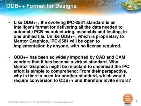
Single File: ODB++ encapsulates all the necessary data in a single file, while Gerber requires multiple files for different layers and features.
-
Intelligent Data Structure: ODB++ uses an intelligent data structure that maintains the relationships between different elements of the PCB design, such as nets and components. Gerber, on the other hand, is a simple image-based format that does not contain such intelligence.
-
Comprehensive Information: ODB++ includes a wider range of information, such as layer stackup, material properties, and design intent, which are not captured in Gerber files.
-
Ease of Use: ODB++ is easier to manage and process, as it eliminates the need for managing multiple files and ensures that all the necessary data is included.
Despite these advantages, Gerber format remains widely used in the industry, particularly for simpler PCB designs or legacy projects. However, the adoption of ODB++ is growing, especially for more complex and high-density PCB designs.
Best Practices for Using ODB++
To ensure smooth and error-free data exchange using ODB++, PCB designers and manufacturers should follow these best practices:
-
Use the Latest Version: Always use the latest version of the ODB++ format supported by your CAD and CAM tools to ensure compatibility and access to the latest features and enhancements.
-
Include All Necessary Data: When exporting an ODB++ file, ensure that all the necessary layers, features, and manufacturing information are included. Incomplete data can lead to delays or errors in the fabrication process.
-
Communicate Design Intent: Use the available options and parameters in your CAD tool to communicate the design intent clearly in the ODB++ file, such as specifying critical dimensions, tolerances, or special requirements.
-
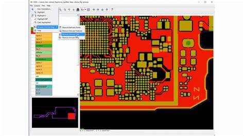
Verify and Validate: Before sending the ODB++ file to the manufacturer, verify and validate the data using the built-in tools in your CAD software or standalone ODB++ viewers. This helps catch any errors or inconsistencies early in the process.
-
Collaborate with Manufacturers: Work closely with your PCB manufacturer and discuss any specific requirements or constraints related to ODB++ data exchange. They can provide guidance on their preferred settings, options, and best practices for using ODB++ in their fabrication process.
Frequently Asked Questions (FAQ)
-
Q: Is ODB++ a proprietary format?
A: While ODB++ was initially developed by Mentor Graphics (now part of Siemens), it is an open format that is widely supported by various CAD and CAM tools in the industry. -
Q: Can ODB++ handle advanced PCB features like embedded components or HDI?
A: Yes, ODB++ supports a wide range of advanced PCB technologies and features, including embedded components, HDI, and rigid-flex designs. -
Q: Do all PCB manufacturers accept ODB++ files?
A: Most modern PCB manufacturers are capable of accepting and processing ODB++ files. However, it is always a good idea to check with your specific manufacturer for their data exchange requirements and preferences. -
Q: Can I use ODB++ for PCB assembly data as well?
A: While ODB++ is primarily used for PCB fabrication data, it can also include some assembly-related information, such as component placement data. However, for full PCB assembly data exchange, other formats like IPC-2581 or ODB++ Design are more commonly used. -
Q: Are there any limitations to using ODB++ for PCB fabrication data exchange?
A: ODB++ is a comprehensive and widely supported format, but there may be some limitations depending on the specific capabilities and requirements of your CAD tool or PCB manufacturer. It is important to discuss any specific limitations or considerations with your tool vendors and manufacturing partners.
Conclusion
ODB++ is a powerful and efficient data exchange format for PCB fabrication, offering numerous benefits over traditional Gerber files. By encapsulating all the necessary design and manufacturing data in a single, intelligent file structure, ODB++ streamlines the communication between PCB designers and manufacturers, reducing errors and improving overall efficiency.
As PCB designs continue to increase in complexity and density, the adoption of ODB++ is likely to grow further. By understanding the structure, benefits, and best practices of using ODB++, PCB designers and manufacturers can leverage this format to enhance their data exchange processes and ensure successful PCB fabrication.

No responses yet