Why Avoiding Ground-Plane Gaps is Critical for Signal Integrity
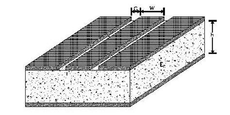
In high-speed printed circuit board (PCB) designs, one of the most important layout rules to follow is to never route a signal trace across a split in the ground plane. A ground-plane gap refers to any break or void in the solid copper ground plane on a PCB layer. Crossing a ground-plane gap with a high-speed signal can severely degrade the signal quality and lead to electromagnetic interference (EMI) issues.
Here are the key reasons why you should avoid crossing ground-plane gaps in your PCB layout:
- Disrupts the Return current path – High-speed signals follow the path of least inductance, which is typically directly under the signal trace in the ground plane. A gap in the ground plane forces the return current to find an alternate path, often with much higher impedance. This disrupts the signal and can cause reflections.
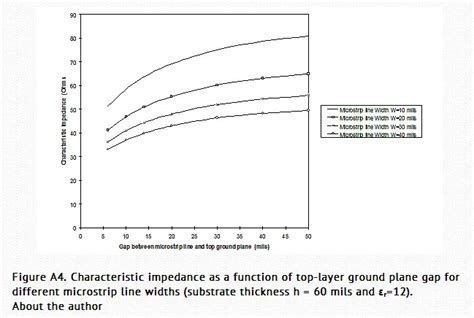
- Creates an uncontrolled impedance discontinuity – When a signal trace crosses a ground plane void, there is an abrupt change in the characteristic impedance of the transmission line. This impedance discontinuity causes a portion of the signal energy to reflect back to the source, distorting the signal.
- Acts as an antenna for EMI – The ground plane gap can act as a slot antenna and radiate noise, causing electromagnetic interference. The length of the gap determines the resonant frequency and the amount of radiation. EMI from gaps can cause a product to fail emissions testing.
- Allows external noise to couple onto signals – Just as the gap can allow signals to radiate outwards as EMI, it can also allow external noise to couple onto the signal lines crossing the gap. This can compromise signal integrity and cause bit errors in digital systems.
Real-World Example of a Ground Plane Gap Issue
To illustrate the impact of crossing a ground plane gap, consider this real-world case study. A designer was developing a high-speed digital camera interface PCB that included an LVDS (low-voltage differential signaling) serial data bus. They noticed that certain camera commands were not being processed reliably.
Upon inspection of the PCB layout, it was discovered that the designer had accidentally routed the LVDS trace pairs across a ground-plane gap created by a slot for an LED indicator. This 2 mm gap caused enough of an impedance discontinuity to distort the 800 Mbps LVDS signals and cause data corruption.
The solution was to re-route the LVDS traces around the slot to maintain a continuous ground reference plane underneath the signals. After this design change, the camera interface worked reliably.
How to Identify and Avoid Ground Plane Gaps in Your PCB Layout
So how can you ensure your high-speed PCB design does not have problematic ground plane gaps? Here are some tips:
- Use your PCB layout tool’s design rule checks (DRCs) – Most modern PCB CAD tools have automated design rule checks that can identify ground plane gaps and flag any traces crossing them. Set up your DRC rules to check for this specific condition.
- Visually inspect your ground plane layer – In addition to automated DRCs, it’s always a good idea to visually review your ground layer for any splits or voids. Use your layout tool’s area fill display mode to clearly see the copper flooding.
- Keep ground vias away from plane edges – Vias that transition between layers can also create gaps in the ground plane if placed too close to the plane edge. Leave enough clearance around vias to avoid fragmenting the ground plane.
- Use stitching vias to bridge gaps when necessary – If a ground plane gap is unavoidable due to other design constraints, you can strategically place stitching vias to bridge the gap and maintain a low-impedance return path. Use as many stitching vias as needed to minimize the return path length.
- Consider using a power plane as a pseudo-ground – If your design has a dedicated power plane layer, you can use it as a low-impedance reference for signals if needed. This is not ideal but can work in a pinch. Make sure the power plane has sufficient decoupling to ground.
PCB Stackup Considerations for Ground Planes
The arrangement of your conductors in your PCB stackup also plays a role in avoiding ground plane gaps. Here are some recommendations:
- Use at least one continuous ground plane in your stackup, preferably near the surface layers where most high-speed signals are routed.
- For multi-layer boards, consider using a stackup with dedicated signal and plane layers. Alternate signal layers with ground planes to provide continuous reference.
- If using a 4-layer board, route all high-speed signals on the top or bottom layers, with the inner layers dedicated as solid ground and power planes.
- Avoid splitting ground planes with large cutouts or slots. If slots are needed for mechanical reasons, try to orient them perpendicular to the signal trace routing direction.
Here is an example 6-layer PCB stackup with good ground plane arrangement:
| Layer | Conductor Type |
|---|---|
| Top | Signal |
| 2 | Ground Plane |
| 3 | Signal |
| 4 | Power Plane |
| 5 | Signal |
| Bottom | Ground Plane |

Measuring the Impact of Ground Plane Gaps
To quantify the impact of a ground plane gap, you can use 3D electromagnetic field solver simulations or actual measurements on a prototype PCB. Here are some common measurements to make:
- TDR (Time Domain Reflectometry) – TDR measurements show impedance changes over the length of a transmission line. A ground plane gap will show up as a sharp impedance spike in the TDR plot. The magnitude of the spike indicates the severity of the discontinuity.
- VNA (Vector Network Analyzer) S-Parameters – VNA measurements show the frequency response of a network. Measuring S11 (return loss) and S21 (insertion loss) of a trace crossing a ground plane gap will show the amount of signal reflection and loss compared to a continuous ground case. Expect to see resonant dips in S21 at frequencies where the gap length is a multiple of a quarter-wavelength.
- Spectrum Analyzer EMI Scans – Doing near-field EMI scans over a powered PCB can reveal “hot spots” of emissions from ground plane gaps. Use a small loop probe connected to a spectrum analyzer and scan over the gap area. Compare this to emissions from solid ground plane regions.
Signal Integrity Simulation Case Study
To illustrate the quantitative impact of a ground plane gap, I simulated a simple microstrip trace crossing a gap using a 2D field solver. The trace was a 50 ohm line, 5 mils wide, over a 5 mil dielectric. The ground gap was 100 mils long.
Here are the S-parameter results, comparing a continuous ground (red) to crossing the gap (blue):
As you can see, the gap causes a significant dip in S21 and spike in S11 around 14 GHz, where the gap length is a quarter-wavelength. The gap reduces transmission by over 5 dB and causes a 10 dB return loss! This shows how severely the gap can distort high frequency signals.

FAQ on Ground Plane Gaps
To recap, here are answers to some frequently asked questions about ground plane gaps in PCB design:
Q: What is a ground plane gap?
A: A ground plane gap is any void or split in the solid copper ground plane of a PCB layer. It’s an area where copper has been removed, either intentionally (for slots, cutouts, etc.) or accidentally (from poor layout).
Q: Why are ground plane gaps bad?
A: Ground plane gaps disrupt the return current path of high-speed signals, causing reflections and EMI radiation. They create impedance discontinuities and allow noise to couple onto signal traces.
Q: How much of a gap is considered problematic?
A: Any gap that is more than a small fraction of a wavelength at the signal frequency can cause issues. A good rule of thumb is to avoid gaps longer than 1/20 of a wavelength. For digital signals, this equates to keeping gaps less than 1/20 of the rise-time length.
Q: Are there any situations where ground plane gaps are acceptable?
A: For low-frequency, low-speed signals (below ~50 MHz), small ground plane gaps may be okay. Power traces can also usually tolerate gaps better than signals. But for any high-speed, high-fidelity signals (e.g. clocks, RF, serial data), you should avoid gaps as much as possible.
Q: How can I fix a design that has ground plane gaps?
A: If you identify ground plane gaps in your PCB layout, first try re-routing traces to avoid crossing the gaps. If that’s not possible, you can try adding stitching vias to bridge the gap. As a last resort, you may need to adjust the placement of components or mechanical cutouts to close the gap.

Conclusion
Avoiding ground plane gaps is a fundamental rule for maintaining signal integrity in high-speed PCB designs. By understanding the impact these gaps can have and following layout best practices to identify and avoid them, you can ensure your high-speed signals stay clean and your product passes EMI testing.
Remember to leverage your PCB layout tool’s automated checking features as well as manual inspection and simulation to verify your ground planes are solid and free of gaps. And if you do run into issues with ground plane gaps, I hope the tips in this article help you find and fix them quickly. Happy PCB designing!

No responses yet