Introduction to PCB CAD
Printed Circuit Board (PCB) design is a complex process that requires the use of specialized software tools known as PCB Computer-Aided Design (CAD) software. These tools allow engineers and designers to create, simulate, and optimize PCB layouts before manufacturing. PCB CAD software has revolutionized the electronics industry by enabling faster, more efficient, and more reliable PCB design processes.
In this article, we will explore the fundamental concepts of PCB design and CAD software, including the key factors that govern PCB designs, the essential features of PCB CAD software, and the best practices for using these tools effectively.
The Importance of PCB Design
PCBs are the backbone of modern electronics. They provide the physical platform for mounting and interconnecting electronic components, such as resistors, capacitors, integrated circuits (ICs), and connectors. The design of a PCB directly affects the performance, reliability, and manufacturability of the final product.
A well-designed PCB should:
- Ensure proper functionality of the electronic circuit
- Minimize electromagnetic interference (EMI) and signal integrity issues
- Facilitate efficient heat dissipation
- Optimize manufacturing costs and time-to-market
To achieve these goals, PCB designers must consider various factors, such as component placement, trace routing, power distribution, and signal integrity. This is where PCB CAD software comes into play.
Key Factors Governing PCB Designs
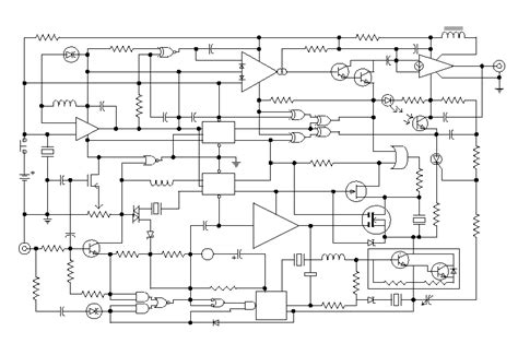
1. Schematic Design
The first step in PCB design is creating a schematic diagram that represents the electrical connections between components. The schematic serves as a blueprint for the PCB layout and helps designers verify the circuit’s functionality before proceeding with the physical design.
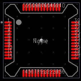
2. Component Placement
Once the schematic is complete, designers must place the components on the PCB layout. Proper component placement is crucial for several reasons:
- Minimizing the distance between connected components to reduce signal delay and power loss
- Ensuring adequate spacing between components to prevent electromagnetic interference and thermal issues
- Facilitating efficient routing of traces and vias
- Optimizing the use of available board space
3. Trace Routing
Trace routing involves creating the conductive paths that connect the components on the PCB. The goal is to route the traces in a way that minimizes signal integrity issues, such as crosstalk, reflections, and electromagnetic interference.
Key considerations for trace routing include:
- Trace width and spacing: Wider traces have lower resistance and can carry more current, but they also occupy more board space. Narrower traces allow for denser routing but may introduce signal integrity issues.
- Trace length matching: In high-speed digital designs, it is essential to match the lengths of traces carrying related signals (e.g., clock and data lines) to minimize signal skew and ensure proper timing.
- Trace impedance: The characteristic impedance of a trace must be controlled to prevent reflections and ensure proper signal transmission. This is particularly important for high-speed signals and controlled impedance designs.
4. Power Distribution
Proper power distribution is essential for ensuring the reliable operation of the electronic circuit. The PCB design must provide a low-impedance, noise-free power supply to all components.
Key considerations for power distribution include:
- Power plane design: The use of power planes (also known as power pours) helps distribute power evenly across the PCB and minimizes voltage drops.
- Decoupling capacitors: Placing decoupling capacitors close to power-hungry components, such as ICs, helps reduce power supply noise and maintains signal integrity.
- Ground plane design: A solid ground plane provides a low-impedance return path for signals and helps minimize electromagnetic interference.
5. Signal Integrity
Signal integrity refers to the ability of a signal to propagate through the PCB without distortion or degradation. Maintaining signal integrity is critical for ensuring the proper functioning of the electronic circuit, especially in high-speed designs.
Key factors that affect signal integrity include:
- Impedance matching: Ensuring that the characteristic impedance of traces matches the impedance of the source and load devices helps prevent reflections and signal distortion.
- Crosstalk: Crosstalk occurs when signals on adjacent traces interfere with each other. Proper trace spacing and the use of guard traces can help minimize crosstalk.
- Reflections: Reflections occur when signals encounter impedance discontinuities, such as vias or connectors. Minimizing reflections requires careful design of transmission lines and the use of termination techniques.

Essential Features of PCB CAD Software
To address the key factors governing PCB designs, modern PCB CAD software offers a wide range of features and tools. Some of the essential features include:
1. Schematic Capture
PCB CAD software provides a schematic editor for creating and editing schematic diagrams. The schematic editor typically includes a library of common electronic components, as well as tools for creating custom components and symbols.
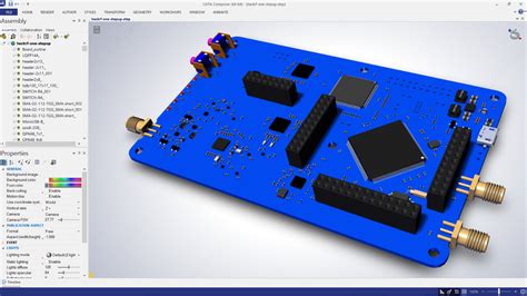
2. PCB Layout
The PCB layout editor is the core of PCB CAD software. It allows designers to place components, route traces, and define board outlines and mounting holes. Advanced PCB layout editors offer features such as:
- Auto-placement and auto-routing: These tools can automatically place components and route traces based on user-defined rules and constraints, saving time and effort.
- Design rule checking (DRC): DRC tools verify that the PCB layout complies with manufacturing and electrical constraints, such as minimum trace width and spacing, hole sizes, and clearances.
- 3D visualization: Many PCB CAD software packages offer 3D rendering capabilities, allowing designers to visualize the PCB assembly and check for mechanical interferences.
3. Simulation and Analysis
To ensure the integrity and reliability of PCB designs, CAD software often includes simulation and analysis tools. These tools allow designers to:
- Perform signal integrity simulations to analyze the behavior of high-speed signals and identify potential issues, such as reflections and crosstalk.
- Conduct thermal analysis to evaluate the temperature distribution across the PCB and identify hot spots that may require additional cooling.
- Analyze power integrity to ensure that the power distribution network can deliver clean, stable power to all components.
4. Manufacturing Output
Once the PCB design is complete, the CAD software generates the necessary manufacturing files, such as Gerber files, drill files, and bill of materials (BOM). These files are used by PCB fabrication and assembly services to manufacture the physical PCB.
Best Practices for Using PCB CAD Software
To make the most of PCB CAD software and ensure successful PCB designs, consider the following best practices:
-
Start with a well-organized schematic: A clean, well-structured schematic is the foundation of a good PCB design. Use hierarchical design techniques and clear labeling to make the schematic easy to understand and maintain.
-
Define design constraints early: Establish the design rules and constraints, such as minimum trace width and spacing, early in the design process. This helps ensure that the PCB layout complies with manufacturing and electrical requirements.
-
Use a consistent component placement strategy: Develop a consistent strategy for placing components on the PCB, taking into account factors such as signal flow, power distribution, and mechanical constraints.
-
Route critical signals first: Begin by routing the most critical signals, such as high-speed clock and data lines, to ensure that they have the optimal path and to minimize interference with other signals.
-
Verify the design with simulation and analysis tools: Use the simulation and analysis tools provided by the PCB CAD software to validate the design and identify potential issues before manufacturing.
-
Collaborate with manufacturers: Work closely with PCB fabrication and assembly services to ensure that the design is manufacturable and to optimize the manufacturing process for cost and reliability.
PCB CAD Software Selection Criteria
Choosing the right PCB CAD software is essential for efficient and effective PCB design. When evaluating PCB CAD software options, consider the following criteria:
-
Ease of use: The software should have a user-friendly interface and intuitive workflows that enable designers to work efficiently.
-
Features and capabilities: Ensure that the software offers the necessary features and tools for your specific design requirements, such as advanced routing capabilities, simulation and analysis tools, and manufacturing output options.
-
Integration with other tools: Consider how well the PCB CAD software integrates with other tools in your design workflow, such as schematic capture software, mechanical CAD (MCAD) software, and version control systems.
-
Scalability: Choose a software package that can scale to accommodate the complexity and size of your PCB designs, both now and in the future.
-
Customer support and community: Look for software vendors that offer reliable customer support and have an active user community, as this can be invaluable for troubleshooting and learning best practices.
Popular PCB CAD Software Packages
The following table compares some of the most popular PCB CAD software packages available on the market:
| Software | Vendor | Key Features |
|---|---|---|
| Altium Designer | Altium | – Advanced routing and placement tools – 3D visualization – Integrated simulation and analysis tools – Extensive component libraries |
| OrCAD | Cadence | – Schematic capture and PCB layout – Constraint-driven design – Signal and power integrity analysis – MCAD integration |
| EAGLE | Autodesk | – Schematic capture and PCB layout – Extensive component libraries – Scripting and customization capabilities |
| KiCad | Open Source | – Free and open-source – Schematic capture and PCB layout – 3D visualization – Integrated with FreeCAD for mechanical design |
Frequently Asked Questions (FAQ)
- What is the difference between schematic capture and PCB layout?
-
Schematic capture involves creating a diagram that represents the electrical connections between components, while PCB layout involves placing components and routing traces on a physical board.
-
What are design rule checks (DRCs) in PCB CAD software?
-
DRCs are automated checks performed by the software to ensure that the PCB layout complies with manufacturing and electrical constraints, such as minimum trace width and spacing, hole sizes, and clearances.
-
How do I ensure signal integrity in high-speed PCB designs?
-
To ensure signal integrity in high-speed designs, use techniques such as impedance matching, minimizing crosstalk, and controlling reflections. PCB CAD software often includes simulation and analysis tools to help identify and resolve signal integrity issues.
-
What are the benefits of using a consistent component placement strategy?
-
A consistent component placement strategy helps minimize signal delay and power loss, ensures adequate spacing between components, facilitates efficient trace routing, and optimizes the use of available board space.
-
How do I choose the right PCB CAD software for my needs?
- When choosing PCB CAD software, consider factors such as ease of use, features and capabilities, integration with other tools, scalability, and customer support. Evaluate your specific design requirements and compare software options based on these criteria.
Conclusion
PCB design and CAD software are essential tools for creating reliable, high-performance electronic products. By understanding the key factors that govern PCB designs, such as schematic design, component placement, trace routing, power distribution, and signal integrity, designers can make informed decisions and optimize their PCB layouts.
To achieve successful PCB designs, it is crucial to choose the right PCB CAD software and follow best practices for using these tools effectively. By selecting software that meets your specific design requirements, collaborating with manufacturers, and continuously learning and refining your skills, you can unlock the full potential of PCB CAD software and create innovative, reliable electronic products.
No responses yet