Introduction to Multilayer PCBs
Multilayer PCBs (Printed Circuit Boards) are essential components in modern electronics, enabling the creation of complex circuits in compact spaces. As technology advances, the demand for more sophisticated and high-performance electronic devices increases, making multilayer PCBs a crucial element in the electronics industry.
What is a Multilayer PCB?
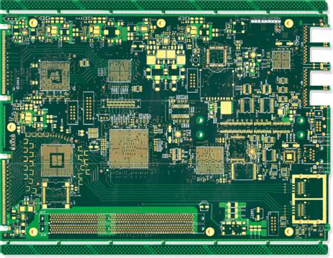
A multilayer PCB is a printed circuit board that consists of three or more conductive copper layers, separated by insulating layers. The conductive layers are interconnected using vias, which are small holes drilled through the board and plated with conductive material. This allows for the creation of complex circuits with a high density of components in a limited space.
Advantages of Multilayer PCBs
Multilayer PCBs offer several advantages over single or double-layer PCBs:
- Space Savings: By stacking multiple layers, multilayer PCBs allow for a higher density of components and circuitry in a smaller footprint.
- Improved Signal Integrity: The use of dedicated ground and power planes in multilayer PCBs helps reduce electromagnetic interference (EMI) and cross-talk, resulting in improved signal integrity.
- Enhanced Reliability: Multilayer PCBs offer better mechanical stability and heat dissipation, which enhances the overall reliability of the electronic device.
- Increased Flexibility: The ability to route signals through multiple layers provides greater flexibility in circuit design and component placement.
Multilayer PCB Structure and Composition
PCB Layers
A typical multilayer PCB consists of the following layers:
- Signal Layers: These are the layers where the actual circuit traces are routed. The number of signal layers depends on the complexity of the circuit and the desired performance.
- Power and Ground Planes: Dedicated layers for power distribution and grounding help maintain signal integrity and reduce EMI.
- Insulating Layers: These layers, typically made of FR-4 or other dielectric materials, separate the conductive layers and provide electrical insulation.
Layer Stack-up
The arrangement of the layers in a multilayer PCB is called the layer stack-up. The stack-up is designed to optimize signal integrity, manufacturability, and cost. A well-designed stack-up ensures proper impedance control, reduces crosstalk, and minimizes EMI.
A common 4-layer PCB stack-up might look like this:
| Layer | Description |
|---|---|
| Top | Signal Layer |
| Inner 1 | Ground Plane |
| Inner 2 | Power Plane |
| Bottom | Signal Layer |
Vias
Vias are small holes drilled through the PCB to interconnect different layers. There are several types of vias:
- Through Hole Vias: These vias go through all layers of the PCB and are used for mounting through-hole components or for connecting signal traces on different layers.
- Blind Vias: These vias connect an outer layer to an inner layer but do not go through the entire board.
- Buried Vias: These vias connect two or more inner layers without reaching the outer layers.

Designing Multilayer PCBs
Design Considerations
When designing a multilayer PCB, several factors must be considered:
- Signal Integrity: Proper routing techniques, such as avoiding sharp corners and minimizing trace lengths, should be employed to maintain signal integrity.
- Impedance Control: The width and spacing of traces, as well as the thickness of the dielectric layers, must be carefully designed to maintain the desired characteristic impedance.
- Crosstalk: Proper spacing between traces and the use of ground planes can help minimize crosstalk between signals.
- Thermal Management: The power dissipation of components and the overall thermal profile of the PCB must be considered to ensure proper heat dissipation.
Design Tools
Several PCB design software tools are available to assist in the creation of multilayer PCBs:
- Altium Designer
- Cadence Allegro
- OrCAD PCB Designer
- KiCad EDA
These tools provide features such as schematic capture, PCB layout, autorouting, and design rule checking (DRC) to ensure the PCB meets the required specifications.
Design Guidelines
When designing multilayer PCBs, following best practices and guidelines can help ensure a successful design:
- Use a grid-based design approach to simplify routing and component placement.
- Follow the manufacturer’s recommended design rules for minimum trace widths, spacings, and via sizes.
- Use ground planes and proper grounding techniques to minimize EMI and improve signal integrity.
- Carefully plan the layer stack-up to optimize signal integrity and manufacturability.
- Perform thorough design reviews and simulations to catch potential issues early in the design process.

Manufacturing Multilayer PCBs
PCB Fabrication Process
The fabrication of multilayer PCBs involves several steps:
- Preparing the Substrate: The base material, typically FR-4, is cut to the desired size and shape.
- Applying the Copper Layers: Copper foil is laminated onto the substrate using heat and pressure.
- Drilling Vias: Holes are drilled through the board for vias and component mounting.
- Plating Vias: The drilled holes are plated with copper to create electrical connections between layers.
- Patterning the Copper Layers: The copper layers are selectively etched to create the desired circuit traces and pads.
- Applying Solder Mask: A protective solder mask is applied to the outer layers to insulate and protect the copper traces.
- Applying Silkscreen: Text and symbols are printed onto the solder mask for component identification and assembly guidance.
- Surface Finishing: A surface finish, such as HASL (Hot Air Solder Leveling) or ENIG (Electroless Nickel Immersion Gold), is applied to the exposed copper areas to protect them from oxidation and enhance solderability.
Quality Control
Ensuring the quality of multilayer PCBs during manufacturing is crucial for the reliability and performance of the final product. Several quality control measures are employed:
- Visual Inspection: Boards are visually inspected for defects such as scratches, dents, or discoloration.
- Automated Optical Inspection (AOI): Machine vision systems are used to detect surface defects, such as missing components or solder bridges.
- Electrical Testing: Continuity and isolation tests are performed to ensure proper electrical connections and the absence of short circuits.
- Microsectioning: Cross-sections of the PCB are examined under a microscope to verify the integrity of vias, plating, and lamination.
- Functional Testing: The assembled PCB is tested under real-world conditions to ensure proper functionality and performance.

Applications of Multilayer PCBs
Consumer Electronics
Multilayer PCBs are widely used in consumer electronics, such as smartphones, tablets, laptops, and wearables. The compact size and high component density enabled by multilayer PCBs allow for the creation of sleek and powerful devices.
Automotive Electronics
The automotive industry relies heavily on multilayer PCBs for various electronic systems, such as engine control units, infotainment systems, and advanced driver assistance systems (ADAS). The robust construction and reliability of multilayer PCBs make them well-suited for the harsh operating conditions in vehicles.
Medical Devices
Multilayer PCBs are essential in medical devices, such as patient monitors, imaging equipment, and implantable devices. The high reliability and signal integrity provided by multilayer PCBs are crucial for ensuring the accurate and safe operation of these life-critical devices.
Industrial Control Systems
Industrial control systems, such as programmable logic controllers (PLCs) and human-machine interfaces (HMIs), utilize multilayer PCBs for their complex circuitry and high-speed communication requirements. The rugged construction of multilayer PCBs allows them to withstand the harsh environments often found in industrial settings.
Frequently Asked Questions (FAQ)
1. What is the difference between a multilayer PCB and a single-layer PCB?
A single-layer PCB has only one conductive layer, while a multilayer PCB has three or more conductive layers separated by insulating layers. Multilayer PCBs offer advantages such as higher component density, improved signal integrity, and better reliability compared to single-layer PCBs.
2. How many layers can a multilayer PCB have?
Multilayer PCBs can have anywhere from four to over thirty layers, depending on the complexity of the circuit and the application requirements. The most common multilayer PCBs have four, six, or eight layers.
3. What materials are used in the construction of multilayer PCBs?
The most common base material for multilayer PCBs is FR-4, a glass-reinforced epoxy laminate. The conductive layers are typically made of copper foil, while the insulating layers are made of prepreg, a partially cured B-stage epoxy resin.
4. How are the layers interconnected in a multilayer PCB?
The layers in a multilayer PCB are interconnected using vias, which are small holes drilled through the board and plated with conductive material. There are three main types of vias: through hole vias, blind vias, and buried vias, each serving different purposes in the interconnection of layers.
5. What are the advantages of using a multilayer PCB over a single-layer PCB?
Multilayer PCBs offer several advantages over single-layer PCBs, including:
– Higher component density and space savings
– Improved signal integrity and reduced electromagnetic interference
– Better mechanical stability and heat dissipation
– Increased design flexibility and routing options
– Enhanced overall reliability and performance
Conclusion
Multilayer PCBs have become an indispensable part of modern electronics, enabling the creation of complex, high-performance devices in compact form factors. By understanding the structure, design considerations, manufacturing processes, and applications of multilayer PCBs, engineers and designers can leverage their advantages to create innovative and reliable electronic products.
As technology continues to advance, the demand for more sophisticated multilayer PCBs will only increase. Staying up-to-date with the latest design tools, manufacturing techniques, and industry best practices will be crucial for success in this rapidly evolving field.
No responses yet