Introduction to Solder Stencils
Solder stencils are an essential tool in the world of Electronics Manufacturing, particularly in surface mount technology (SMT). These thin, precisely cut metal sheets allow for the accurate and consistent application of Solder Paste onto printed Circuit Boards (PCBs). Solder paste is a mixture of tiny solder particles suspended in a flux medium, which helps to establish electrical and mechanical connections between components and the PCB.
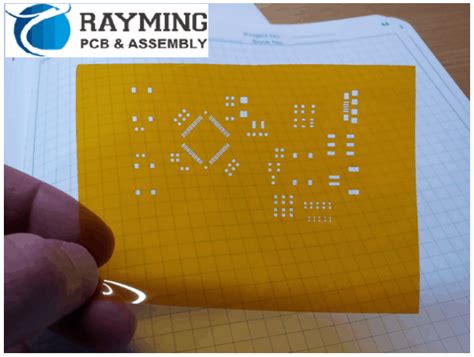
What are Solder Stencils?
Solder stencils are typically made from stainless steel or nickel-coated brass and feature apertures (openings) that correspond to the pads on a PCB where solder paste needs to be applied. The thickness of the stencil determines the amount of solder paste deposited, which is crucial for ensuring proper soldering and preventing defects such as bridging or insufficient solder joints.
Why Use Solder Stencils?
Using solder stencils offers several advantages over manual solder paste application methods:
-
Consistency: Stencils ensure a uniform amount of solder paste is applied to each pad, reducing the likelihood of defects caused by too much or too little solder.
-
Efficiency: Stencils allow for the rapid application of solder paste to multiple pads simultaneously, significantly reducing the time required for assembly.
-
Precision: Well-designed stencils enable the accurate placement of solder paste, even on tiny pads or fine-pitch components.
-
Scalability: Stencils are essential for high-volume production, as they enable the consistent application of solder paste across large numbers of PCBs.
Types of Solder Stencils
There are several types of solder stencils, each with its own characteristics and applications.
Laser-Cut Stencils
Laser-cut stencils are created using a high-precision laser to cut apertures into a metal sheet. This process allows for the creation of highly accurate and detailed stencils, making them suitable for fine-pitch components and complex PCB Designs. Laser-cut stencils are more durable than chemically etched stencils and can be made from a variety of materials, including stainless steel and nickel-coated brass.
Chemically Etched Stencils
Chemically etched stencils are made by selectively removing material from a metal sheet using a chemical etching process. This method is less precise than laser cutting but is generally more affordable for larger apertures and simpler PCB designs. Chemically etched stencils are typically made from stainless steel and have a shorter lifespan compared to laser-cut stencils.
Electroformed Stencils
Electroformed stencils are created by electroplating nickel onto a master template, which is then removed, leaving a thin, precise stencil. This process allows for the creation of highly detailed stencils with smooth aperture walls, making them ideal for fine-pitch applications. However, electroformed stencils are more expensive and less durable than laser-cut or chemically etched stencils.
3D-Printed Stencils
3D-printed stencils are a relatively new development in the world of solder paste application. These stencils are created using additive manufacturing techniques, such as fused deposition modeling (FDM) or stereolithography (SLA). While 3D-printed stencils are not as durable as metal stencils, they offer the advantage of rapid prototyping and customization, making them suitable for low-volume production or testing purposes.

Designing Solder Stencils
Designing an effective solder stencil requires careful consideration of several factors, including PCB layout, component types, and solder paste properties.
Aperture Design
Aperture design is crucial for ensuring the proper amount of solder paste is applied to each pad. The size and shape of the apertures should be based on the size and shape of the pads on the PCB, as well as the type of components being used.
Aperture Width and Length
The width and length of the apertures should be slightly larger than the corresponding pads on the PCB to allow for some misalignment during the solder paste application process. A general rule of thumb is to make the apertures 10-20% larger than the pads.
Aperture Shape
The shape of the apertures should match the shape of the pads on the PCB. Common aperture shapes include rectangular, square, and circular. For fine-pitch components or densely populated PCBs, custom aperture shapes may be necessary to ensure adequate solder paste coverage without causing bridging.
Stencil Thickness
The thickness of the solder stencil determines the amount of solder paste deposited onto the pads. Thicker stencils deposit more solder paste, while thinner stencils deposit less. The optimal stencil thickness depends on several factors, including the size and pitch of the components, the desired solder joint profile, and the properties of the solder paste.
| Component Pitch | Recommended Stencil Thickness |
|---|---|
| > 0.65 mm | 150 – 200 μm |
| 0.5 – 0.65 mm | 120 – 150 μm |
| 0.4 – 0.5 mm | 100 – 120 μm |
| < 0.4 mm | 80 – 100 μm |
Stencil Material
The choice of stencil material depends on the desired durability, cost, and precision of the stencil. Stainless steel is the most common material for solder stencils due to its durability and resistance to wear. Nickel-coated brass stencils offer similar durability but are less expensive than stainless steel. For high-precision applications, electroformed nickel stencils may be necessary to achieve the required level of detail and accuracy.

Manufacturing Solder Stencils
Once the solder stencil design is finalized, the stencil can be manufactured using one of the methods described earlier: laser cutting, chemical etching, electroforming, or 3D printing.
Laser Cutting
Laser cutting is the most common method for manufacturing solder stencils. The process involves using a high-powered laser to cut the apertures into a metal sheet. Laser cutting offers several advantages, including high precision, rapid turnaround times, and the ability to create complex aperture shapes.
Chemical Etching
Chemical etching involves selectively removing material from a metal sheet using a chemical etching solution. This process is less precise than laser cutting but is more affordable for larger apertures and simpler designs. Chemical etching is typically used for stencils with apertures larger than 0.1 mm.
Electroforming
Electroforming is a process that involves electroplating nickel onto a master template, which is then removed, leaving a thin, precise stencil. This method is used for creating high-precision stencils with smooth aperture walls, making them ideal for fine-pitch applications. However, electroforming is more expensive and time-consuming than laser cutting or chemical etching.
3D Printing
3D printing is a relatively new method for manufacturing solder stencils. This process involves using additive manufacturing techniques, such as FDM or SLA, to create a stencil from a digital model. 3D-printed stencils are not as durable as metal stencils but offer the advantage of rapid prototyping and customization.

Using Solder Stencils
Once the solder stencil is manufactured, it can be used to apply solder paste to the PCB. The process involves the following steps:
-
Alignment: The solder stencil is aligned with the PCB using fiducial markers or alignment pins to ensure proper registration between the stencil apertures and the pads on the PCB.
-
Solder Paste Application: Solder paste is dispensed onto the stencil and spread across the surface using a squeegee or automated solder paste printer. The solder paste fills the apertures in the stencil, depositing a precise amount onto each pad.
-
Stencil Removal: After the solder paste is applied, the stencil is carefully removed, leaving the solder paste deposits on the PCB pads.
-
Component Placement: The components are then placed onto the solder paste deposits using manual or automated pick-and-place equipment.
-
Reflow Soldering: The PCB is heated in a reflow oven, causing the solder paste to melt and form a permanent electrical and mechanical connection between the components and the PCB.
Maintaining Solder Stencils
Proper maintenance of solder stencils is essential for ensuring consistent solder paste application and preventing defects. Some key maintenance practices include:
-
Cleaning: Solder stencils should be cleaned regularly to remove excess solder paste and prevent clogging of the apertures. Cleaning can be done using solvents, ultrasonic cleaners, or specialized stencil cleaning equipment.
-
Inspection: Regular inspection of the stencil for damage, wear, or clogged apertures is essential for maintaining print quality. Damaged or worn stencils should be repaired or replaced as necessary.
-
Storage: When not in use, solder stencils should be stored in a clean, dry environment to prevent damage and contamination. Stencils should be stored flat or hung vertically to prevent warping.
Frequently Asked Questions (FAQ)
-
What is the difference between a solder stencil and a solder screen?
A solder stencil is a thin, metal sheet with apertures that allow solder paste to be deposited onto specific areas of a PCB. A solder screen, on the other hand, is a mesh screen with a patterned emulsion that allows solder paste to be pushed through onto the PCB. Stencils are more common in modern SMT assembly due to their higher precision and durability. -
How often should I clean my solder stencil?
The frequency of cleaning depends on several factors, including the type of solder paste used, the volume of production, and the environment in which the stencil is used. As a general rule, solder stencils should be cleaned at least once per shift or every 1,000 prints, whichever comes first. However, more frequent cleaning may be necessary for high-volume production or when using certain types of solder paste. -
Can I reuse a damaged solder stencil?
It depends on the extent and type of damage. Minor damage, such as small nicks or dents, may be repairable using laser welding or chemical filling techniques. However, if the damage is extensive or affects the apertures, it is generally recommended to replace the stencil to ensure consistent solder paste application and prevent defects. -
What is the typical lifespan of a solder stencil?
The lifespan of a solder stencil depends on several factors, including the material, thickness, and frequency of use. Laser-cut stainless steel stencils can typically withstand 50,000 to 100,000 prints before needing to be replaced, while chemically etched stencils may last for 10,000 to 30,000 prints. Electroformed nickel stencils have a shorter lifespan, typically around 5,000 to 10,000 prints. -
Can I use the same solder stencil for different PCB designs?
No, each PCB design requires a unique solder stencil that matches the layout and component placement of that specific design. Using the wrong stencil can result in incorrect solder paste application, leading to defects such as bridging, insufficient solder joints, or component misalignment.
Conclusion
Solder stencils play a critical role in the SMT assembly process, enabling the precise and consistent application of solder paste to PCBs. By understanding the different types of stencils, design considerations, manufacturing processes, and maintenance practices, engineers and technicians can ensure high-quality solder paste printing and minimize defects in their assemblies.
As electronics continue to become smaller and more complex, the importance of solder stencils will only continue to grow. By staying up-to-date with the latest developments in stencil technology and best practices, manufacturers can maintain a competitive edge and produce reliable, high-performance electronic devices.
No responses yet