Introduction to Laser Depaneling
Laser depaneling is a precise and efficient method for separating individual printed circuit boards (PCBs) from a larger panel. This process is particularly useful when dealing with delicate or intricate PCB designs, such as round Ceramic PCBs. In this article, we will explore the benefits of laser depaneling, the challenges associated with depaneling round ceramic PCBs, and the steps involved in the laser depaneling process.
What is Laser Depaneling?
Laser depaneling is a process that uses a focused laser beam to cut through the material connecting individual PCBs on a larger panel. This method offers several advantages over traditional mechanical depaneling techniques, such as:
- Increased precision
- Reduced stress on the PCB
- Minimal debris generation
- Faster processing times
Benefits of Laser Depaneling for Round Ceramic PCBs
Round ceramic PCBs present unique challenges when it comes to depaneling due to their shape and material properties. Laser depaneling offers several benefits that make it an ideal choice for this type of PCB:
- Precise cutting along curved edges
- Minimal thermal stress on the ceramic material
- Reduced risk of cracking or chipping
- Ability to handle thin and fragile substrates
Challenges of Depaneling Round Ceramic PCBs
Material Properties
Ceramic PCBs are made from a combination of ceramic and metal layers, which can be more brittle and prone to cracking than traditional FR-4 PCBs. This makes them more susceptible to damage during the depaneling process.
Curved Edges
The round shape of these PCBs can make it difficult to achieve clean, precise cuts using mechanical depaneling methods. Laser depaneling, on the other hand, can easily follow the curved contours of the board.
Thermal Stress
Ceramic materials are sensitive to thermal stress, which can cause cracking or warping if not managed properly during the depaneling process. Laser depaneling minimizes thermal stress by focusing the heat on a small area and allowing for rapid cooling.

Laser Depaneling Process for Round Ceramic PCBs
Step 1: Panel Design and Preparation
To ensure successful laser depaneling, the PCB panel must be designed with appropriate spacing and support structures. This includes:
- Adding adequate spacing between individual boards
- Incorporating break-away tabs or mousebites
- Ensuring proper fiducial placement for alignment
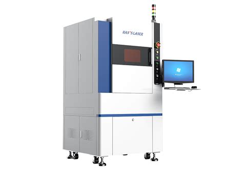
Step 2: Laser System Setup
The laser system must be properly configured to handle the specific requirements of round ceramic PCBs. This involves:
- Selecting the appropriate laser type and power settings
- Adjusting the focus and spot size of the laser beam
- Setting up the motion control system for accurate positioning
Step 3: Alignment and Fixturing
Precise alignment is critical for achieving accurate cuts and minimizing damage to the PCBs. This step includes:
- Utilizing fiducials for panel alignment
- Securing the panel in a dedicated fixture
- Verifying the alignment using machine vision or other techniques
Step 4: Laser Cutting
Once the panel is aligned and secured, the laser cutting process can begin. The laser beam follows the predetermined cut path, vaporizing the material connecting the individual PCBs. Key considerations during this step include:
- Maintaining consistent cutting speed and power
- Monitoring the process for any signs of thermal stress or damage
- Implementing proper ventilation and fume extraction
Step 5: Post-Processing and Inspection
After the laser cutting is complete, the individual PCBs must be cleaned and inspected for any signs of damage or defects. This may involve:
- Removing any residual debris or dust
- Visually inspecting the cut edges for smoothness and accuracy
- Performing electrical tests to verify functionality

Advantages of Laser Depaneling for Round Ceramic PCBs
| Advantage | Description |
|---|---|
| Precision | Laser depaneling offers high precision, allowing for clean, accurate cuts along curved edges. |
| Reduced Stress | The focused laser beam minimizes thermal and mechanical stress on the delicate ceramic material. |
| Flexibility | Laser systems can easily adapt to different PCB shapes, sizes, and layouts. |
| Speed | Laser depaneling offers faster processing times compared to mechanical methods. |
| Cost-effectiveness | The precision and speed of laser depaneling can lead to reduced material waste and improved production efficiency. |

Frequently Asked Questions (FAQ)
1. What type of laser is used for depaneling round ceramic PCBs?
CO2 lasers and UV lasers are commonly used for depaneling ceramic PCBs. CO2 lasers are suitable for thicker substrates, while UV lasers offer higher precision for thinner materials.
2. Can laser depaneling be used for other types of PCBs?
Yes, laser depaneling can be used for a wide range of PCB materials, including FR-4, aluminum-backed, and flexible circuits.
3. How does laser depaneling compare to mechanical depaneling in terms of cost?
While laser depaneling systems may have a higher initial investment cost, they can offer long-term cost savings through increased precision, reduced material waste, and faster processing times.
4. What safety precautions are necessary when using laser depaneling systems?
Proper eye protection, such as safety glasses or goggles designed for the specific laser wavelength, must be worn. Adequate ventilation and fume extraction are also essential to remove any harmful particles or gases generated during the laser cutting process.
5. Can laser depaneling be automated for high-volume production?
Yes, laser depaneling systems can be integrated into automated production lines, enabling high-volume processing with consistent quality and minimal operator intervention.
Conclusion
Laser depaneling is a powerful technique for separating round ceramic PCBs from larger panels. By offering precision, flexibility, and reduced stress on the delicate ceramic material, laser depaneling overcomes the challenges associated with traditional mechanical methods. When properly implemented, laser depaneling can lead to improved production efficiency, reduced material waste, and higher-quality end products.
As the demand for miniaturized, high-performance electronic devices continues to grow, the use of laser depaneling for round ceramic PCBs and other advanced substrates will likely become increasingly common in the electronics manufacturing industry.
No responses yet