What is Kicad?
Kicad is a free, open-source, cross-platform software for designing electronic schematics and printed circuit boards (PCBs). It provides an integrated environment for schematic capture, PCB layout, and design rule checking. Kicad runs on Windows, Linux and macOS.
The main components of the Kicad software suite include:
| Component | Description |
|---|---|
| Eeschema | Schematic editor and component editor |
| Pcbnew | PCB layout editor and footprint editor |
| GerbView | Gerber viewer |
| Pcb Calculator | Calculator for components, track width, etc. |
| Pl Editor | Page layout editor |
Together, these tools enable a complete electronic design workflow from concept to manufacturing.
Installing Kicad
To get started, first download and install Kicad from the official website: https://www.kicad.org/download/
Kicad is available for Windows, Linux, and macOS. Follow the installation instructions for your operating system. The installation package includes all the necessary components.

Kicad Workflow Overview
The typical workflow in Kicad consists of the following steps:
- Create a new project
- Design the schematic in Eeschema
- Assign footprints to components
- Generate a netlist
- Layout the PCB in Pcbnew
- Run design rule checks
- Generate manufacturing files
Let’s go through each of these steps in more detail.

Creating a New Project
To create a new project in Kicad:
- Open the Kicad project manager
- Click File > New Project > New Project
- Choose a name and location for your project
- Select the default schematics and PCB layouts
- Click OK
This will create a new project directory with the following structure:
- MyProject/
  - MyProject.kicad_pcb
  - MyProject.kicad_sch
  - MyProject.kicad_wks
  - MyProject.pretty/
  - MyProject.sch
The .sch file is the schematic, .kicad_pcb is the PCB layout, .kicad_sch stores schematic settings, .kicad_wks stores page layout settings, and the .pretty directory contains footprints.

Designing the Schematic
The first step in designing a circuit is creating the schematic. The schematic defines the components and the connections between them.
To create a schematic:
- In the Kicad project manager, double-click on the
.schfile to open it in Eeschema - You will see a blank schematic sheet
- Add components using the Place Symbol tool on the right toolbar
- Search for the desired component in the popup dialog and select it
- Place the components on the schematic sheet by left-clicking
- Draw wires between the pins of components using the Place Wire tool
- Add net labels, power ports, and I/O ports using the corresponding tools
- Add a title and date, rev ID, and page number using the drawing tools
- Annotate the schematic to update component designators and pin numbers (Tools > Annotate Schematic)
- Run an Electrical Rules Check (Inspect > Electrical Rules Check)
- Save the schematic
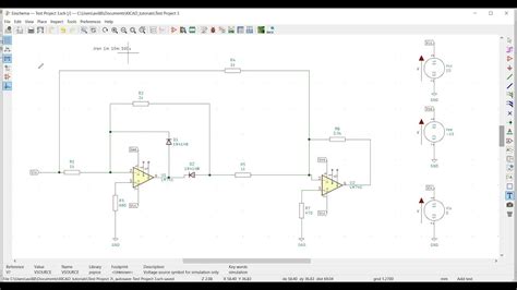
Here’s an example of a simple schematic in Kicad:
Assigning Footprints
After creating the schematic, the next step is to assign footprints to each component. A footprint defines the physical layout and dimensions of a component on the PCB.
To assign footprints:
- In Eeschema, open the schematic
- Run the Annotate tool (Tools > Annotate Schematic) if you haven’t already
- Click on a component to select it
- Press the “e” key to open the Symbol Properties dialog
- In the Footprint field, enter the name of an existing footprint or press the “…” button to open the footprint library
- Select the desired footprint
- Repeat steps 3-6 for each component
- Save the schematic
Kicad comes with a large library of built-in footprints. You can also create your own custom footprints in the Footprint Editor.
Generating Netlists
A netlist is a text file that describes the connectivity between components in the schematic. The netlist is used to transfer design information from the schematic to the PCB layout.
To generate a netlist:
- In Eeschema, open the schematic
- Make sure you have assigned footprints to all components
- Click Tools > Generate Netlist File
- Select “Pcbnew” as the netlist format
- Choose an output directory and filename
- Click Generate
- The netlist will be saved as a
.netfile
Laying Out the PCB
With the schematic and netlist complete, you are ready to layout the PCB. PCB layout involves placing components, routing traces, adding copper zones, and defining the board outline.
To layout a PCB:
- In the Kicad project manager, double-click on the
.kicad_pcbfile to open Pcbnew - You will see a blank PCB layout view
- Import the netlist (File > Import > Netlist)
- Select the netlist file you generated in the previous step
- Components will appear on the PCB
- Arrange the components by dragging and dropping
- Place key components first (connectors, switches, large ICs, etc.)
- Align components to an underlying grid
- Add mounting holes for fasteners
- Define the board outline using the Edge Cuts layer
- Add copper fills for power and ground using the Add Filled Zones tool
- Route traces between pads using the Route Tracks tool
- Adjust track width for power traces
- Add vias to change routing layers
- Ensure adequate clearances between components, traces, and board edges
- Run a Design Rules Check (Inspect > Design Rules Checker)
- Generate 3D models to preview the final board
- Save the PCB layout
Here’s an example of a PCB layout in progress in Pcbnew:
Design Rule Checking
Design Rule Checking (DRC) is an automated check to verify that your PCB layout meets manufacturing constraints and design rules. DRC will check for errors such as overlapping traces, insufficient clearances, missing connections, etc.
To run a Design Rules Check:
- In Pcbnew, open the PCB layout
- Configure the design rules (File > Board Setup > Design Rules)
- Set constraints for clearances, track widths, via sizes, etc.
- Click OK to close the dialog
- Run the Design Rules Check (Inspect > Design Rules Checker)
- View the DRC report and correct any errors
- Rerun DRC until the layout passes all checks
Properly configuring the design rules from the start will help avoid time-consuming errors later in the design process. Refer to your PCB manufacturer’s capabilities and guidelines when setting up the design rules.
Generating Manufacturing Files
The final step is generating the files needed for PCB manufacturing. These files tell the fabrication house how to manufacture and assemble your PCB.
The main files used in PCB manufacturing include:
| File Type | Extension | Description |
|---|---|---|
| Gerber | .gbr, .gm1 |
Contains layer images (copper, mask, silkscreen, etc.) |
| NC Drill | .drl |
Contains drill hole locations and sizes |
| Pick and Place | .pos |
Contains component locations for automated assembly |
| Bill of Materials | .csv, .xls |
List of components used in the design |
| Assembly Drawing | .pdf |
Drawing showing component placement |
| Fab Drawing | .pdf |
Drawing with dimensions and specs for the bare board |
To generate manufacturing files in Kicad:
- In Pcbnew, open the PCB layout
- Run a Design Rules Check to ensure the layout is error-free
- Click File > Fabrication Outputs
- Select “Gerber” as the plot format
- Click Plot to generate Gerber files
- Select “Excellon” as the drill format
- Click Generate Drill File to create the NC drill file
- Generate the Pick and Place file (File > Fabrication Outputs > Footprint Position (.pos) File)
- Create the Bill of Materials (File > Fabrication Outputs > BOM)
- Export 3D models (File > Export > STEP) for mechanical integration
Package these files and send them to your PCB manufacturer for fabrication and assembly. Including detailed fab and assembly drawings will help avoid mistakes.
PCB Assembly and Bringing Up
After receiving your fabricated PCBs, you will need to assemble and test them. PCB assembly involves soldering components to the board. For low volume assembly, this can be done by hand. Use a soldering iron, solder, and tweezers to carefully solder each component.
Proper technique is important to avoid bridging pins, cold joints, or damaging components. Always use a temperature-controlled soldering iron and lead-free solder. Refer to the assembly drawing to ensure each component is in the correct place and orientation.
After assembly, power up the board and test its functionality. Check for shorts, opens, and proper voltage levels. Use a multimeter and oscilloscope to debug any issues.
If the board doesn’t work as expected, double-check the schematic and PCB layout for errors. Common issues include swapped components, incorrect pinouts, missing connections, and insufficient power supply decoupling.
Careful design, assembly, and testing will result in a functional PCB ready for integration into your project.
Kicad Best Practices and Tips
Here are some best practices and tips to keep in mind when working with Kicad:
- Use a consistent naming scheme for components, nets, and footprints
- Place decoupling capacitors close to ICs
- Use copper fills for improved power delivery and EMI reduction
- Avoid acute angles in traces to reduce reflections
- Keep different signal types separated (analog, digital, power, etc.)
- Use ground planes whenever possible
- Make traces as short and direct as possible
- Minimize vias, especially on high-speed signals
- Follow the datasheet recommendations for component footprints and pinouts
- Simulate and analyze critical circuits before laying out the PCB
- Keep your libraries organized and up to date
- Backup your project files regularly
- Refer to the official Kicad documentation and tutorials for more information
KiCad Tutorial FAQs
What are the minimum system requirements for Kicad?
Kicad can run on relatively modest hardware. The minimum recommended system requirements are:
- 1 GHz processor
- 2 GB RAM
- 5 GB disk space
- 1024×768 display resolution
- GPU with OpenGL support
Is Kicad really free? What’s the catch?
Yes, Kicad is completely free and open-source software released under the GNU GPL v3 license. There are no hidden fees, restricted features, or trial periods. The source code is available on GitHub for anyone to view, modify, and contribute to.
Can I design multi-layer PCBs in Kicad?
Yes, Kicad supports designing multi-layer PCBs. There is no hard limit on the number of layers, but realistically most designs will use 2 to 4 layers. More layers are possible but require careful stackup design and consideration for manufacturability.
Does Kicad include simulation tools?
Kicad does not include a built-in simulator. However, it can generate SPICE netlists for use in external simulators such as ngspice and LTspice. There are also third-party plugins and tools that add simulation features to Kicad.
How can I get help if I’m stuck using Kicad?
There are several resources available for getting help with Kicad:
- The official Kicad documentation and user manual
- The Kicad forums and mailing lists
- The Kicad subreddit (/r/kicad)
- Electronics StackExchange
- YouTube tutorials and walkthroughs
Asking questions and searching for answers online is a great way to overcome roadblocks and expand your skills.
Conclusion
Kicad is a powerful, open-source tool for designing electronic schematics and PCBs. With an integrated workflow, extensive component libraries, and active community support, Kicad enables electronics enthusiasts and professionals to bring their projects from concept to reality.
This Kicad tutorial covered the fundamental concepts and steps involved in using Kicad, including:
- Installing Kicad
- Creating a project
- Designing a schematic
- Assigning footprints
- Generating netlists
- Laying out a PCB
- Running design rule checks
- Generating manufacturing files
- Assembling and testing the PCB
By following the workflow and best practices outlined here, you’ll be well on your way to designing successful PCBs using Kicad. As with any skill, practice and persistence are key. Don’t be afraid to experiment, make mistakes, and learn from the experience.
For more information on using Kicad, consult the official documentation, tutorials, and community resources. With time and effort, you’ll be designing complex, professional-quality PCBs using Kicad.
No responses yet