What is KiCad?
KiCad is a cross-platform EDA software suite that includes several tools for designing electronic circuits:
- Eeschema: Schematic capture editor
- Pcbnew: PCB layout editor
- GerbView: Gerber file viewer
- Cvpcb: Footprint selector
- Bitmap2Component: Convert images to footprints
KiCad is known for its user-friendly interface, extensive component libraries, and active community support.
Getting Started with KiCad
Installation
To begin using KiCad, you’ll need to download and install the software on your computer. Visit the official KiCad website (https://www.kicad.org/) and download the appropriate version for your operating system (Windows, macOS, or Linux). Follow the installation instructions provided.
Creating a New Project
Once you have KiCad installed, launch the application and create a new project:
- Click on “File” > “New Project” or press Ctrl+N.
- Choose a location for your project and give it a name.
- Click “Save” to create the project.
KiCad will create a new project folder containing several files, including a schematic file (.sch) and a PCB layout file (.kicad_pcb).

Designing the Schematic
Adding Components
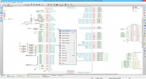
- Double-click the .sch file in the project folder to open Eeschema.
- Press the “Place Symbol” button (A) or press the ‘a’ key to add components to your schematic.
- Search for the desired component in the library browser and click “OK” to place it on the schematic.
- Repeat this process for all the components in your circuit.
Connecting Components
- Press the “Place Wire” button (W) or press the ‘w’ key to start drawing wires between component pins.
- Click on the starting pin, then click on the ending pin to create a connection.
- To create a junction (a connection between crossing wires), press ‘j’ or click the “Place Junction” button.
Labeling and Annotating
- Press the “Place Text” button (T) or press the ‘t’ key to add labels and annotations to your schematic.
- Click on the schematic to place the text and enter your desired label or annotation.
- Use the “Place Global Label” (Shift+L) and “Place Local Label” (L) buttons to create hierarchical labels for multi-sheet schematics.
Assigning Footprints
- Click on the “Assign Footprints” button (F) or press the ‘f’ key to open Cvpcb.
- For each component, select an appropriate footprint from the available libraries.
- Click “Apply” and then “Close” to save the footprint assignments.

PCB Layout
Importing the Netlist
- Switch to the PCB layout editor by double-clicking the .kicad_PCB File in the project folder.
- Click on “Tools” > “Update PCB from Schematic” to import the netlist from your schematic.
Placing Components
- Press the ‘p’ key or click the “Place Footprints” button to start placing components on the PCB.
- Arrange the components in a logical manner, considering factors such as signal flow, component size, and board dimensions.
- Use the ‘r’ key to rotate components and the ‘f’ key to flip them.
Routing Traces
- Press the ‘x’ key or click the “Route Tracks” button to start routing traces between component pads.
- Left-click to start a trace, and left-click again to change direction or end the trace.
- Use the ‘v’ key to switch between routing layers (e.g., top and bottom).
- Press ‘Alt’ while routing to create a via, which allows a trace to switch between layers.
Adding Copper Fills and Zones
- Press the ‘a’ key or click the “Add Filled Zone” button to create a copper fill or zone.
- Click to define the zone outline, and right-click to close the outline.
- Set the zone properties, such as net name, layer, and clearance, in the “Copper Zone Properties” dialog.
Design Rule Checking (DRC)
- Click on “Tools” > “DRC” to open the Design Rules Checker.
- Configure the design rules according to your PCB manufacturer’s specifications.
- Run the DRC to identify any design rule violations and fix them accordingly.

Manufacturing
Generating Gerber Files
- Click on “File” > “Plot” to open the plot dialog.
- Select the “Gerber” format and choose the layers you want to export (e.g., F.Cu, B.Cu, F.SilkS, etc.).
- Click “Plot” to generate the Gerber files.
Generating Drill Files
- Click on “File” > “Fabrication Outputs” > “Drill Files” to open the drill file generator.
- Configure the drill file settings according to your PCB manufacturer’s requirements.
- Click “Generate Drill File” to create the drill files.
Sending Files to Manufacturer
- Compress the Gerber and drill files into a single archive (e.g., .zip).
- Send the archive to your chosen PCB manufacturer for fabrication.
Frequently Asked Questions (FAQ)
-
Is KiCad really free?
Yes, KiCad is free and open-source software, released under the GNU General Public License (GPL). -
Can I use KiCad for commercial projects?
Absolutely. KiCad can be used for both personal and commercial projects without any limitations. -
Does KiCad support multi-sheet schematics?
Yes, KiCad supports hierarchical, multi-sheet schematics, making it suitable for complex designs. -
Can I import designs from other EDA software into KiCad?
KiCad can import designs from several other EDA packages, such as Eagle and Altium Designer, using third-party tools or plugins. -
Is there a community forum for KiCad users?
Yes, there is an active community forum (https://forum.kicad.info/) where users can ask questions, share their designs, and get support from experienced KiCad users and developers.
| Feature | Description |
|---|---|
| Cross-platform | KiCad runs on Windows, macOS, and Linux |
| Schematic capture | Create and edit electronic schematics using Eeschema |
| PCB layout | Design and route printed circuit boards using Pcbnew |
| Component library | Extensive built-in component library and user-created parts |
| Netlisting | Generate netlists for PCB layout and simulation |
| Design rule checking | Built-in DRC for detecting design rule violations |
| Gerber and drill files | Generate industry-standard files for PCB fabrication |
| Multi-sheet schematics | Support for hierarchical, multi-sheet schematic designs |
| Scripting and automation | Python scripting for automating tasks and creating plugins |
In conclusion, KiCad is a powerful and user-friendly EDA software that allows beginners and experienced designers alike to create professional-grade electronic circuits. By following this step-by-step KiCad Tutorial, you should now have a solid foundation for designing your own PCBs. Remember to explore the extensive documentation, community forums, and online resources to further expand your KiCad knowledge and skills. Happy designing!
No responses yet