What is PCB impedance Matching?
Printed Circuit Board (PCB) impedance matching is the process of designing transmission lines on a PCB to have the same characteristic impedance as the components they are connecting. The goal is to minimize reflections and standing waves caused by impedance mismatches, which can degrade signal integrity, especially at high frequencies.
Impedance matching is critical in high-speed digital circuits, RF circuits, and any application where signal integrity is important. By matching the impedance of the transmission lines to the source and load impedances, maximum power transfer can be achieved, and signal reflections can be minimized.
Types of Transmission Lines
There are several types of transmission lines used in PCB Design, each with its own characteristics and applications:
-
Microstrip: A microstrip is a transmission line consisting of a conductive trace on one side of a dielectric substrate, with a ground plane on the opposite side. Microstrips are commonly used in PCB design due to their simplicity and ease of fabrication.
-
Stripline: A stripline is a transmission line consisting of a conductive trace embedded within a dielectric substrate, with ground planes on both sides. Striplines offer better shielding and lower radiation compared to microstrips but are more complex to fabricate.
-
Coplanar Waveguide (CPW): A coplanar waveguide consists of a conductive trace with ground planes on either side, all on the same side of the dielectric substrate. CPWs offer lower dispersion and better control over impedance compared to microstrips and striplines.
| Transmission Line | Advantages | Disadvantages |
|---|---|---|
| Microstrip | Simple, easy to fabricate | Higher radiation, less shielding |
| Stripline | Better shielding, lower radiation | More complex to fabricate |
| Coplanar Waveguide | Lower dispersion, better impedance control | Requires more board space |
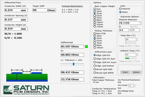
Calculating Characteristic Impedance
To achieve impedance matching, it is necessary to calculate the characteristic impedance of the transmission lines. The characteristic impedance depends on the geometry of the transmission line and the properties of the dielectric substrate.
Microstrip Characteristic Impedance
The characteristic impedance of a microstrip can be calculated using the following formula:
Z0 = (87 / √(εr + 1.41)) * ln(5.98 * h / (0.8 * w + t))
Where:
– Z0 is the characteristic impedance in ohms
– εr is the relative permittivity of the dielectric substrate
– h is the thickness of the dielectric substrate in mm
– w is the width of the conductive trace in mm
– t is the thickness of the conductive trace in mm
Stripline Characteristic Impedance
The characteristic impedance of a stripline can be calculated using the following formula:
Z0 = (60 / √εr) * ln(4 * b / (0.67 * π * (0.8 * w + t)))
Where:
– Z0 is the characteristic impedance in ohms
– εr is the relative permittivity of the dielectric substrate
– b is the distance between the ground planes in mm
– w is the width of the conductive trace in mm
– t is the thickness of the conductive trace in mm
Coplanar Waveguide Characteristic Impedance
The characteristic impedance of a coplanar waveguide can be calculated using the following formula:
Z0 = (30 * π) / (√εeff) * (K(k) / K(k’))
Where:
– Z0 is the characteristic impedance in ohms
– εeff is the effective permittivity of the dielectric substrate
– K(k) and K(k’) are complete elliptic integrals of the first kind
– k = w / (w + 2 * s)
– k’ = √(1 – k^2)
– w is the width of the conductive trace in mm
– s is the gap between the conductive trace and the ground planes in mm
Impedance Matching Techniques
There are several techniques used to achieve impedance matching in PCB design:
-
Termination Resistors: Termination resistors can be used to match the impedance of the transmission line to the load impedance. The value of the termination resistor should be equal to the characteristic impedance of the transmission line.
-
Stub Matching: Stub matching involves adding a short or open-circuited transmission line (stub) to the main transmission line to cancel out reflections. The length and impedance of the stub are chosen to provide the desired matching.
-
Quarter-wave transformers: A quarter-wave transformer is a transmission line with a length of one-quarter wavelength at the operating frequency and an impedance that is the geometric mean of the source and load impedances. Quarter-wave transformers can be used to match impedances over a narrow frequency range.
-
Tapered Lines: Tapered lines are transmission lines with a gradually changing width, which can be used to match impedances over a wide frequency range. The impedance of the tapered line varies smoothly from the source impedance to the load impedance.
| Matching Technique | Advantages | Disadvantages |
|---|---|---|
| Termination Resistors | Simple, effective at low frequencies | Power dissipation, not suitable for high frequencies |
| Stub Matching | Effective at high frequencies, no power dissipation | Requires additional board space, narrow bandwidth |
| Quarter-Wave Transformers | Simple, effective over narrow bandwidth | Narrow bandwidth, requires precise length control |
| Tapered Lines | Wide bandwidth, smooth impedance transition | Requires more board space, complex to design |

Zero Resistance Impedance Matching
Zero resistance impedance matching is a technique used to achieve perfect impedance matching by eliminating the need for termination resistors. This is done by designing the transmission line to have a characteristic impedance equal to the load impedance.
Benefits of Zero Resistance Impedance Matching
-
No Power Dissipation: Since there are no termination resistors, there is no power dissipation, which can be significant in high-power applications.
-
Improved Signal Integrity: Perfect impedance matching eliminates reflections and standing waves, resulting in improved signal integrity and reduced signal distortion.
-
Simplified Design: Zero resistance impedance matching simplifies PCB design by eliminating the need for termination resistors and matching networks.
Designing for Zero Resistance Impedance Matching
To achieve zero resistance impedance matching, the following steps should be followed:
-
Determine the load impedance: The first step is to determine the impedance of the load, which could be an antenna, a transceiver, or any other component.
-
Choose the appropriate transmission line: Based on the operating frequency, board space constraints, and other factors, choose the appropriate type of transmission line (microstrip, stripline, or coplanar waveguide).
-
Calculate the characteristic impedance: Using the formulas provided earlier, calculate the characteristic impedance of the chosen transmission line to match the load impedance.
-
Adjust the geometry of the transmission line: Modify the width and thickness of the conductive trace, the thickness of the dielectric substrate, and other geometrical parameters to achieve the desired characteristic impedance.
-
Simulate and optimize: Use electromagnetic simulation tools to model the transmission line and optimize its performance. Make adjustments as necessary to achieve the best possible impedance match.
FAQ
-
Q: What is the purpose of impedance matching in PCB design?
A: The purpose of impedance matching is to minimize reflections and standing waves caused by impedance mismatches, which can degrade signal integrity, especially at high frequencies. By matching the impedance of the transmission lines to the source and load impedances, maximum power transfer can be achieved, and signal reflections can be minimized. -
Q: What are the different types of transmission lines used in PCB design?
A: The three main types of transmission lines used in PCB design are microstrip, stripline, and coplanar waveguide (CPW). Microstrips are the simplest and most common, consisting of a conductive trace on one side of a dielectric substrate, with a ground plane on the opposite side. Striplines offer better shielding and lower radiation, but are more complex to fabricate. CPWs offer lower dispersion and better control over impedance, but require more board space. -
Q: How do you calculate the characteristic impedance of a transmission line?
A: The characteristic impedance of a transmission line depends on its geometry and the properties of the dielectric substrate. For a microstrip, the characteristic impedance can be calculated using the formula Z0 = (87 / √(εr + 1.41)) * ln(5.98 * h / (0.8 * w + t)), where εr is the relative permittivity of the substrate, h is the substrate thickness, w is the trace width, and t is the trace thickness. Similar formulas exist for striplines and CPWs. -
Q: What are some common impedance matching techniques used in PCB design?
A: Common impedance matching techniques include termination resistors, stub matching, quarter-wave transformers, and tapered lines. Termination resistors are simple and effective at low frequencies, but dissipate power and are not suitable for high frequencies. Stub matching is effective at high frequencies and does not dissipate power, but requires additional board space and has a narrow bandwidth. Quarter-wave transformers are simple and effective over a narrow bandwidth, but require precise length control. Tapered lines offer a wide bandwidth and smooth impedance transition, but require more board space and are complex to design. -
Q: What are the benefits of zero resistance impedance matching?
A: Zero resistance impedance matching offers several benefits, including no power dissipation, improved signal integrity, and simplified design. By eliminating the need for termination resistors, zero resistance impedance matching avoids the power dissipation associated with them, which can be significant in high-power applications. Perfect impedance matching also eliminates reflections and standing waves, resulting in improved signal integrity and reduced signal distortion. Finally, zero resistance impedance matching simplifies PCB design by eliminating the need for termination resistors and matching networks.
Conclusion
Impedance matching is a critical aspect of PCB design, particularly in high-speed digital circuits, RF circuits, and any application where signal integrity is important. By matching the impedance of transmission lines to the source and load impedances, reflections and standing waves can be minimized, and maximum power transfer can be achieved.
There are several types of transmission lines used in PCB design, including microstrips, striplines, and coplanar waveguides, each with its own advantages and disadvantages. The characteristic impedance of these transmission lines can be calculated using formulas that depend on their geometry and the properties of the dielectric substrate.
Common impedance matching techniques include termination resistors, stub matching, quarter-wave transformers, and tapered lines. Each technique has its own strengths and weaknesses, and the choice of technique depends on the specific requirements of the application.
Zero resistance impedance matching is a technique that offers several benefits, including no power dissipation, improved signal integrity, and simplified design. By designing the transmission line to have a characteristic impedance equal to the load impedance, perfect impedance matching can be achieved without the need for termination resistors or matching networks.
In conclusion, impedance matching is a vital skill for PCB Designers, and a good understanding of the principles and techniques involved is essential for creating high-performance, reliable electronic systems. By following the guidelines and best practices presented in this article, designers can effectively match impedances and ensure optimal signal integrity in their PCB designs.
No responses yet