Introduction to PCB Impedance
Printed Circuit Board (PCB) impedance is a crucial factor in ensuring the integrity and reliability of high-speed electronic circuits. As signal frequencies continue to increase, the importance of controlling and managing PCB impedance becomes even more critical. In this article, we will delve into the concepts of impedance calculation and explore the cross-section features that influence PCB layout design.
What is PCB Impedance?
PCB impedance refers to the opposition to the flow of alternating current (AC) in a PCB trace. It is a complex quantity that combines resistance, capacitance, and inductance. The characteristic impedance of a PCB trace is determined by its physical dimensions, dielectric properties of the substrate material, and the frequency of the signal being transmitted.
Why is PCB Impedance Important?
Controlling PCB impedance is essential for several reasons:
-
Signal Integrity: Proper impedance matching ensures that signals propagate through the PCB traces without excessive reflections or distortions. Mismatched impedances can lead to signal integrity issues, such as ringing, overshoot, and undershoot.
-
Power Integrity: Impedance control helps maintain stable power delivery to components on the PCB. Fluctuations in power supply voltage can cause signal integrity problems and affect the overall performance of the circuit.
-
Electromagnetic Compatibility (EMC): Controlling impedance reduces electromagnetic interference (EMI) and improves the electromagnetic compatibility of the PCB. Properly designed impedance-controlled traces minimize unwanted radiation and crosstalk between signals.
Impedance Calculation Techniques
To achieve accurate impedance control, designers must calculate the target impedance values for PCB traces. There are several methods and formulas used for impedance calculation, depending on the trace geometry and dielectric properties.
Microstrip Impedance Calculation
Microstrip is a common PCB trace geometry where the signal trace is placed on the top layer of the PCB, with a ground plane on the bottom layer. The characteristic impedance of a microstrip trace can be calculated using the following formula:
Z₀ = (87 / √(ɛᵣ + 1.41)) * ln(5.98 * h / (0.8 * w + t))
Where:
– Z₀ is the characteristic impedance in ohms (Ω)
– ɛᵣ is the relative dielectric constant of the substrate material
– h is the thickness of the dielectric (substrate) in mils
– w is the width of the trace in mils
– t is the thickness of the trace in mils
Stripline Impedance Calculation
Stripline is another common PCB trace geometry where the signal trace is sandwiched between two ground planes. The characteristic impedance of a stripline trace can be calculated using the following formula:
Z₀ = (60 / √ɛᵣ) * ln(4 * h / (0.67 * (0.8 * w + t)))
Where the variables have the same meanings as in the microstrip formula.
Coplanar Waveguide Impedance Calculation
Coplanar waveguide (CPW) is a trace geometry where the signal trace is flanked by ground planes on the same layer. The characteristic impedance of a CPW trace can be calculated using the following formula:
Z₀ = (30π / √ɛᵣ) * (K(k’) / K(k))
Where:
– K(k) and K(k’) are complete elliptic integrals of the first kind
– k = S / (S + 2W)
– k’ = √(1 – k²)
– S is the spacing between the signal trace and ground planes
– W is the width of the signal trace
Cross Section Features in PCB Layout
The cross-section of a PCB plays a vital role in determining the impedance and signal integrity characteristics. Let’s explore some key cross-section features and their impact on PCB layout.
Dielectric Thickness
The thickness of the dielectric material (substrate) between the signal trace and the reference plane affects the characteristic impedance. A thicker dielectric results in higher impedance, while a thinner dielectric leads to lower impedance. Designers must carefully select the appropriate dielectric thickness to achieve the desired impedance values.
Trace Width and Thickness
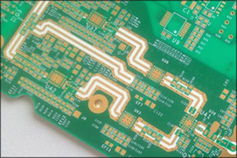
The width and thickness of the signal trace directly influence the characteristic impedance. Wider traces have lower impedance, while narrower traces have higher impedance. Similarly, thicker traces exhibit lower impedance compared to thinner traces. Designers must balance the trace dimensions to meet the target impedance requirements while considering manufacturing limitations and current-carrying capacity.
Spacing between Traces
The spacing between adjacent traces affects the coupling capacitance and crosstalk. Adequate spacing must be maintained to minimize unwanted interactions between signals. The spacing requirements depend on factors such as signal rise times, dielectric properties, and the sensitivity of the circuits to crosstalk.
Ground Plane Considerations
The presence and placement of ground planes in the PCB cross-section are crucial for impedance control and signal integrity. Continuous ground planes provide a low-impedance return path for high-frequency signals and help shield against external noise. Designers should ensure proper grounding strategies, such as using ground planes on adjacent layers and implementing ground vias near signal traces.

PCB Stack-up Design
The PCB stack-up refers to the arrangement of conductive layers and dielectric materials in the cross-section of the board. Proper stack-up design is essential for achieving the desired impedance and ensuring signal integrity.
Signal Layer Arrangement
Signal layers should be strategically placed within the stack-up to minimize the distance between the signal traces and their respective reference planes. This reduces loop inductance and improves signal integrity. High-speed signals are often routed on inner layers to take advantage of the shielding provided by the adjacent ground planes.
Power and Ground Plane Placement
Power and ground planes should be placed close to the signal layers to provide a low-impedance power distribution network and minimize the loop area for return currents. Designers should consider using dedicated power and ground planes for different voltage domains to reduce noise coupling.
Dielectric Material Selection
The choice of dielectric material significantly affects the impedance and signal propagation characteristics. Common PCB substrate materials include FR-4, Rogers, and Isola. Each material has its own dielectric constant (ɛᵣ) and loss tangent (tanδ), which influence the impedance and signal attenuation. Designers should select the appropriate dielectric material based on the frequency range, cost, and performance requirements of the application.
Impedance Simulation and Verification
To ensure that the designed PCB meets the target impedance values, designers often rely on simulation tools and verification techniques.
Impedance Simulation Tools
Electronic Design Automation (EDA) tools, such as Cadence Allegro, Mentor Graphics HyperLynx, and Altium Designer, offer impedance simulation capabilities. These tools allow designers to model the PCB stack-up, define trace geometries, and simulate the impedance behavior. Simulation results provide insight into the expected impedance values and help identify any potential issues before fabrication.
Time-Domain Reflectometry (TDR)
Time-Domain Reflectometry (TDR) is a measurement technique used to verify the actual impedance of fabricated PCBs. TDR involves sending a fast-rising signal through the PCB trace and analyzing the reflections caused by impedance discontinuities. By comparing the measured impedance profile with the target values, designers can validate the impedance control and identify any manufacturing or design issues.
FAQ
1. What is the difference between microstrip and stripline impedance?
Microstrip and stripline are two common PCB trace geometries. In microstrip, the signal trace is on the top layer, with a ground plane on the bottom layer. In stripline, the signal trace is sandwiched between two ground planes. Microstrip impedance is typically higher than stripline impedance for the same dielectric thickness and trace dimensions.
2. How does the dielectric constant affect PCB impedance?
The dielectric constant (ɛᵣ) of the substrate material directly influences the characteristic impedance of PCB traces. A higher dielectric constant results in lower impedance, while a lower dielectric constant leads to higher impedance. Designers must consider the dielectric constant when selecting substrate materials and calculating impedance values.
3. What is the purpose of ground planes in PCB layout?
Ground planes serve multiple purposes in PCB layout. They provide a low-impedance return path for high-frequency signals, minimizing loop inductance and improving signal integrity. Ground planes also help shield signals from external noise and reduce electromagnetic interference (EMI). Additionally, they contribute to power integrity by providing a stable reference voltage.
4. How can I minimize crosstalk between PCB traces?
Crosstalk between PCB traces can be minimized through several techniques:
– Increase the spacing between adjacent traces to reduce coupling capacitance.
– Use ground planes to shield signals and provide isolation.
– Route sensitive signals on different layers to minimize coupling.
– Utilize differential signaling techniques for high-speed interfaces.
– Implement proper grounding and power distribution strategies.
5. What are the challenges in designing high-speed PCBs with impedance control?
Designing high-speed PCBs with impedance control presents several challenges:
– Achieving accurate impedance calculations and simulations.
– Managing signal integrity issues, such as reflections, crosstalk, and attenuation.
– Ensuring proper power integrity and minimizing power supply noise.
– Dealing with manufacturing tolerances and variations in material properties.
– Balancing cost, performance, and manufacturability constraints.
Conclusion
PCB Impedance Control is a critical aspect of high-speed electronic design. By understanding impedance calculation techniques and the impact of cross-section features, designers can create robust and reliable PCBs. Proper impedance control ensures signal integrity, power integrity, and electromagnetic compatibility.
To achieve optimal results, designers should carefully consider factors such as trace geometries, dielectric properties, and stack-up design. Simulation tools and verification methods, such as TDR, help validate the impedance characteristics and identify any issues before fabrication.
As signal frequencies continue to rise and PCB designs become more complex, mastering impedance control techniques becomes increasingly important. By following best practices and staying up-to-date with the latest design methodologies, engineers can overcome the challenges associated with high-speed PCB design and deliver products that meet the demanding requirements of modern electronic systems.
No responses yet