What is an IC Substrate?
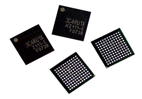
An integrated circuit (IC) substrate, also known as a chip carrier or package substrate, is the foundation upon which a semiconductor chip or die is mounted. It serves as an intermediary connection between the tiny circuitry of the chip and the larger circuitry of the printed circuit board (PCB). The substrate plays a crucial role in the performance, reliability, and functionality of the integrated circuit package.
IC substrates are typically made from a dielectric material, such as bismaleimide triazine (BT) resin or polyimide, with embedded conductive traces and vias for electrical connections. They come in various form factors and configurations to accommodate different chip sizes, pin counts, and package types.
Importance of IC Substrates
IC substrates are essential components in the semiconductor packaging process for several reasons:
-
Electrical Interconnection: The substrate provides electrical pathways between the chip and the PCB through conductive traces, vias, and solder balls or pins.
-
Mechanical Support: It offers mechanical support and protection to the delicate semiconductor die, ensuring its integrity during handling, testing, and assembly.
-
Thermal Management: The substrate helps dissipate heat generated by the chip, preventing thermal-related failures and improving the overall reliability of the package.
-
Signal Integrity: A well-designed substrate minimizes signal distortion, crosstalk, and impedance mismatch, ensuring high-speed and reliable signal transmission between the chip and the PCB.
-
Packaging Density: Advanced substrate technologies enable higher-density interconnects and smaller package sizes, allowing for more compact and efficient electronic devices.

Types of IC Substrates
There are several types of IC substrates, each with its own characteristics and applications:
1. Laminate Substrates
Laminate substrates are the most common type of IC substrates, widely used in Ball Grid Array (BGA), Pin Grid Array (PGA), and Land Grid Array (LGA) packages. They are made by stacking and laminating multiple layers of dielectric material (e.g., BT resin) and copper foils, which are then patterned and etched to form the required circuitry.
Laminate substrates offer good mechanical strength, thermal stability, and electrical performance at a relatively low cost. They are suitable for a wide range of applications, from consumer electronics to industrial and automotive systems.
2. Ceramic Substrates
Ceramic substrates are made from inorganic materials, such as alumina (Al2O3) or aluminum nitride (AlN), which offer excellent thermal conductivity, high-temperature stability, and low dielectric loss. They are commonly used in high-performance, high-reliability applications, such as aerospace, defense, and high-power electronics.
Ceramic substrates can be further classified into two sub-types:
a. High-Temperature Co-fired Ceramic (HTCC): HTCC substrates are fabricated by co-firing multiple layers of ceramic material and metal (e.g., tungsten or molybdenum) at temperatures above 1,600°C. They offer high thermal conductivity and are suitable for hermetic packaging.
b. Low-Temperature Co-fired Ceramic (LTCC): LTCC substrates are made by co-firing ceramic layers and metal (e.g., silver or gold) at temperatures below 1,000°C. They provide good electrical performance, low dielectric loss, and the ability to integrate passive components, such as resistors and capacitors, within the substrate.
3. Flex Substrates
Flex substrates, also known as flexible printed circuits (FPCs), are made from thin, flexible dielectric materials, such as polyimide or polyester, with patterned conductive traces. They offer high flexibility, lightweight, and the ability to conform to various shapes and sizes, making them ideal for applications with limited space or require bendability, such as wearables, smartphones, and medical devices.
Flex substrates can be further categorized into two types:
a. Single-sided Flex: Single-sided flex substrates have conductive traces on only one side of the dielectric material, offering the most basic level of flexibility and interconnection.
b. Double-sided Flex: Double-sided flex substrates have conductive traces on both sides of the dielectric material, providing higher interconnect density and more complex routing capabilities.

Manufacturing Process of IC Substrates
The manufacturing process of IC substrates involves several key steps:
-
Material Preparation: The dielectric material (e.g., BT resin or polyimide) and conductive material (e.g., copper foil) are prepared and conditioned for the substrate fabrication process.
-
Lamination: Multiple layers of dielectric material and conductive foils are stacked and laminated together under high temperature and pressure to form a solid substrate panel.
-
Drilling: Through-holes and vias are drilled into the substrate panel using mechanical or laser drilling techniques to create vertical interconnections between layers.
-
Patterning: The desired circuitry pattern is transferred onto the conductive layers using photolithography and etching processes, removing unwanted copper and leaving behind the required traces and pads.
-
Plating: The through-holes and vias are plated with conductive material (e.g., copper) to establish electrical connections between layers.
-
Solder Mask Application: A protective solder mask layer is applied to the substrate surface, exposing only the areas intended for soldering, such as pads and solder balls.
-
Surface Finishing: The exposed pads and contacts are plated with a surface finish material, such as Electroless Nickel Immersion Gold (ENIG), Organic Solderability Preservative (OSP), or Immersion Tin, to enhance solderability and protect against oxidation.
-
Singulation: The substrate panel is cut into individual substrate units using a dicing saw or laser cutting equipment, ready for the chip assembly process.

Advanced IC Substrate Technologies
As the demand for higher performance, smaller form factors, and increased functionality in electronic devices grows, several advanced IC substrate technologies have emerged to address these challenges:
1. Through-Silicon Via (TSV) Substrates
TSV substrates incorporate vertical interconnections that pass completely through the silicon die, enabling 3D chip stacking and shorter signal paths. This technology offers higher interconnect density, improved signal integrity, and reduced power consumption compared to traditional wire bonding or flip-chip packaging.
TSV substrates are commonly used in high-performance applications, such as 3D integrated circuits, memory stacks, and advanced packaging solutions like 2.5D and 3D IC integration.
2. Embedded Passive and Active Devices
Some advanced IC substrates incorporate embedded passive components, such as resistors, capacitors, and inductors, directly within the substrate layers. This integration reduces the need for discrete components on the PCB, saving space and improving electrical performance.
In addition, active devices, such as transistors and diodes, can also be embedded into the substrate using advanced packaging techniques like fan-out wafer-level packaging (FOWLP) or chip-on-wafer-on-substrate (CoWoS). These technologies enable the creation of highly integrated and compact system-in-package (SiP) solutions.
3. High-Density Interconnect (HDI) Substrates
HDI substrates feature finer line widths, smaller via sizes, and higher layer counts compared to conventional laminate substrates. They enable higher routing density, improved signal integrity, and reduced package size, making them suitable for advanced applications like 5G communications, high-performance computing, and artificial intelligence (AI) processors.
HDI substrates often incorporate microvias, which are small, laser-drilled vias that interconnect adjacent layers, allowing for more efficient use of substrate space and enabling higher-density designs.
Challenges and Future Trends
Despite the advancements in IC substrate technologies, several challenges and future trends are shaping the industry:
-
Cost Reduction: As the demand for high-performance and miniaturized electronic devices increases, there is a constant pressure to reduce the cost of IC substrates without compromising on quality and reliability.
-
Material Innovations: The development of new dielectric materials with improved thermal, mechanical, and electrical properties is crucial to meet the ever-increasing requirements of advanced packaging solutions.
-
Environmental Considerations: The need for environmentally friendly and sustainable IC substrate materials and manufacturing processes is driving the adoption of halogen-free, lead-free, and recyclable solutions.
-
5G and High-Speed Applications: The proliferation of 5G networks and high-speed data transmission is driving the demand for IC substrates with enhanced signal integrity, low latency, and high bandwidth capabilities.
-
Heterogeneous Integration: The trend towards heterogeneous integration, which involves the integration of multiple dies with different functionalities on a single substrate, is gaining traction. This requires advanced substrate technologies that can accommodate diverse die sizes, materials, and interconnect requirements.
-
Wafer-Level Packaging: The adoption of wafer-level packaging (WLP) techniques, where the substrate is fabricated directly on the wafer before singulation, is increasing. WLP offers higher interconnect density, smaller package sizes, and lower cost compared to traditional substrate-based packaging.
FAQ
1. What is the difference between a laminate and a ceramic IC substrate?
Laminate substrates are made from organic dielectric materials, such as BT resin or polyimide, and offer good mechanical strength, thermal stability, and electrical performance at a lower cost. Ceramic substrates, on the other hand, are made from inorganic materials, such as alumina or aluminum nitride, and provide excellent thermal conductivity, high-temperature stability, and low dielectric loss, making them suitable for high-performance and high-reliability applications.
2. What are the advantages of using a flex substrate?
Flex substrates offer several advantages, including high flexibility, lightweight, and the ability to conform to various shapes and sizes. They are ideal for applications with limited space or that require bendability, such as wearables, smartphones, and medical devices. Flex substrates also enable the creation of more compact and efficient electronic packages.
3. What is the role of solder mask in IC substrates?
The solder mask is a protective layer applied to the surface of the IC substrate, exposing only the areas intended for soldering, such as pads and solder balls. It serves several purposes:
a. Insulation: The solder mask prevents accidental short circuits between adjacent traces and pads.
b. Protection: It protects the substrate surface from oxidation, contamination, and mechanical damage during handling and assembly.
c. Solder Control: The solder mask defines and contains the solder on the desired areas, preventing solder bridging and ensuring reliable solder joints.
4. What are the benefits of using TSV substrates?
TSV (Through-Silicon Via) substrates offer several benefits compared to traditional packaging technologies:
a. Higher Interconnect Density: TSVs enable vertical interconnections through the silicon die, allowing for higher interconnect density and more compact package sizes.
b. Improved Signal Integrity: Shorter signal paths provided by TSVs result in reduced signal delay, lower power consumption, and improved overall signal integrity.
c. 3D Integration: TSV technology enables 3D chip stacking, allowing for the creation of highly integrated and efficient 3D IC packages with enhanced functionality and performance.
5. What are the challenges in adopting advanced IC substrate technologies?
The adoption of advanced IC substrate technologies comes with several challenges:
a. Cost: Advanced substrate technologies, such as TSVs, HDI, and embedded devices, often involve higher manufacturing costs due to the increased complexity and precision required in the fabrication process.
b. Reliability: Ensuring the reliability and long-term performance of advanced substrates under various environmental conditions and operating stresses is crucial, requiring extensive testing and qualification.
c. Design Complexity: Designing for advanced substrates requires specialized knowledge and tools to address signal integrity, thermal management, and manufacturing constraints effectively.
d. Supply Chain: The availability and sourcing of advanced substrate materials, equipment, and expertise can be a challenge, especially for smaller companies or those new to the technology.
Despite these challenges, the adoption of advanced IC substrate technologies is essential to meet the ever-increasing demands for higher performance, smaller form factors, and enhanced functionality in modern electronic devices.
No responses yet