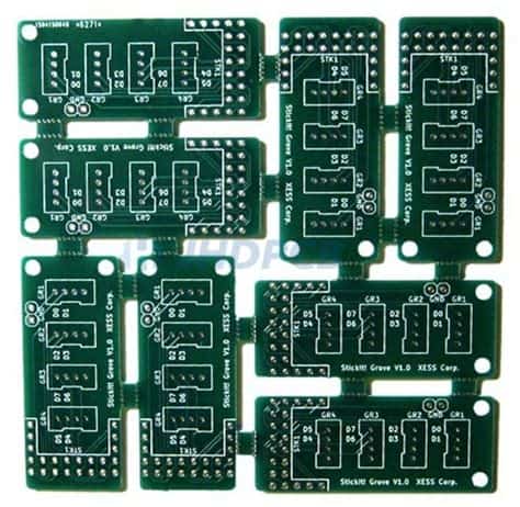
What is PCB Panelization?
PCB panelization is the process of grouping multiple printed circuit board designs onto a single panel for manufacturing. This technique is used to optimize the production process, reduce costs, and increase efficiency. By panelizing PCBs, manufacturers can produce a larger number of boards in a single run, minimizing the time and resources required for setup and handling.
Benefits of PCB Panelization
- Cost reduction
- Increased production efficiency
- Simplified handling and assembly
- Consistent quality across multiple boards
CAM (Computer-Aided Manufacturing) in PCB Panelization
CAM software plays a crucial role in the PCB panelization process. It allows designers and manufacturers to create, optimize, and manage panelization layouts efficiently. CAM tools provide a range of features and functionality to streamline the panelization workflow, ensuring accurate and reliable results.
Key Features of CAM Software for PCB Panelization
- Panel layout creation and editing
- Automatic and manual placement of PCB designs
- Optimization of panel utilization
- Generation of manufacturing files (Gerber, drill, etc.)
- Design rule checking (DRC) and error detection
Step-by-Step Guide to Panelizing PCBs with CAM
Step 1: Preparing the PCB Design Files
Before starting the panelization process, ensure that your PCB design files are complete and ready for manufacturing. This includes:
- Schematic and PCB layout files
- Bill of Materials (BOM)
- Assembly drawings and instructions
- Gerber files and drill files
Step 2: Importing PCB Design Files into CAM Software
- Launch your CAM software and create a new project.
- Import the Gerber files and drill files for each PCB design that you want to panelize.
- Verify that the imported files are correctly aligned and free of errors.
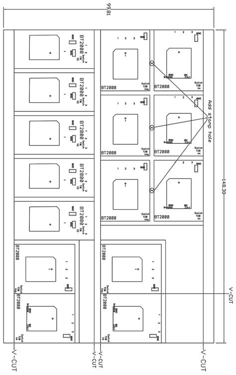
Step 3: Creating the Panel Layout
- Define the panel size and shape based on your manufacturing requirements and constraints.
- Place the imported PCB designs onto the panel, considering factors such as spacing, orientation, and registration marks.
- Optimize the panel layout to maximize material utilization and minimize waste.
- Add any necessary fiducial marks, tooling holes, or other features required for manufacturing.
Step 4: Applying Design Rules and Constraints
- Set up design rules and constraints specific to your manufacturing process, such as minimum spacing, copper thickness, and drill sizes.
- Run a Design Rule Check (DRC) to ensure that your panel layout complies with the specified rules and constraints.
- Make any necessary adjustments to the panel layout to resolve any DRC violations or errors.
Step 5: Generating Manufacturing Files
- Once your panel layout is finalized, generate the necessary manufacturing files, such as Gerber files, drill files, and assembly drawings.
- Review the generated files to ensure they are complete and accurate.
- Package the manufacturing files and send them to your PCB manufacturer for production.

Best Practices for PCB Panelization with CAM
- Optimize panel utilization to minimize material waste and reduce costs.
- Ensure adequate spacing between PCB designs to prevent manufacturing issues.
- Use consistent and clear naming conventions for files and layers.
- Incorporate fiducial marks and tooling holes for accurate registration and assembly.
- Communicate clearly with your PCB manufacturer to ensure that your panelization requirements are understood and met.
Common Challenges and Solutions in PCB Panelization
| Challenge | Solution |
|---|---|
| Insufficient spacing between PCB designs | Adjust the panel layout to ensure adequate spacing and clearance. |
| Inconsistent or missing fiducial marks | Incorporate standardized fiducial marks in the panel layout and verify their presence and accuracy. |
| Inefficient material utilization | Optimize the panel layout to maximize the number of PCB designs per panel and minimize waste. |
| Incorrect or incomplete manufacturing files | Double-check the generated files and ensure they include all necessary information for production. |
| Communication issues with the PCB manufacturer | Establish clear communication channels and provide detailed specifications and requirements. |
Frequently Asked Questions (FAQ)
1. What is the minimum spacing required between PCB designs on a panel?
The minimum spacing between PCB designs on a panel depends on various factors, such as the manufacturing process, board thickness, and copper weight. Consult with your PCB manufacturer to determine the appropriate spacing for your specific project.
2. Can I panelize PCBs with different thicknesses or copper weights?
While it is possible to panelize PCBs with different thicknesses or copper weights, it is generally recommended to keep these properties consistent within a single panel. This ensures optimal manufacturing results and reduces the risk of issues during production.
3. How do I determine the optimal panel size for my PCB designs?
The optimal panel size depends on several factors, including the dimensions of your PCB designs, the available manufacturing equipment, and the desired production quantity. Work closely with your PCB manufacturer to determine the most suitable panel size for your project.
4. What are fiducial marks, and why are they important in PCB panelization?
Fiducial marks are reference points placed on the PCB panel that help align and orient the board during the manufacturing process. They ensure accurate registration and placement of components, reducing the risk of assembly errors and improving overall quality.
5. Can I panelize PCBs with different designs on the same panel?
Yes, it is possible to panelize PCBs with different designs on the same panel, as long as they share similar manufacturing specifications and requirements. This approach can help optimize production and reduce costs, especially for low-volume or prototype builds.
Conclusion
PCB panelization is a critical step in the manufacturing process, enabling efficient and cost-effective production of printed circuit boards. By leveraging CAM software and following best practices, designers and manufacturers can create optimal panel layouts that maximize material utilization, minimize waste, and ensure consistent quality across multiple PCB designs.
By understanding the key principles of PCB panelization and working closely with experienced PCB manufacturers, you can streamline your production process, reduce costs, and achieve reliable results for your electronic projects.
No responses yet