Introduction to KiCad and Gerber Files
KiCad is a free and open-source electronic design automation (EDA) software that allows users to create schematic diagrams and printed circuit board (PCB) layouts. It has gained popularity among hobbyists and professionals alike due to its powerful features and user-friendly interface. Once a PCB Design is complete in KiCad, it needs to be exported to Gerber files for manufacturing.
Gerber files are the industry standard format for PCB fabrication. They contain all the necessary information required by PCB manufacturers to produce the physical board, including the copper layers, solder mask, silkscreen, and drill data. Exporting your KiCad PCB design to Gerber files is a crucial step in the PCB fabrication process.
In this article, we will guide you through the process of exporting your KiCad PCB to Gerber files, ensuring that your design is ready for manufacturing. We will cover the following topics:
- Preparing Your KiCad PCB for Export
- Generating Gerber Files in KiCad
- Verifying and Inspecting Gerber Files
- Common Issues and Troubleshooting
- Best Practices for Gerber File Generation
- Frequently Asked Questions (FAQ)
Preparing Your KiCad PCB for Export
Before exporting your KiCad PCB to Gerber files, it is essential to ensure that your design is complete and error-free. Follow these steps to prepare your PCB for export:
Design Rule Check (DRC)
Run a Design Rule Check (DRC) on your PCB layout to identify any design violations or potential issues. KiCad’s DRC tool checks your design against a set of predefined rules and constraints, such as minimum trace width, clearance, and hole size. To run a DRC:
- Open your PCB layout in KiCad’s PCB Editor.
- Click on the “Tools” menu and select “DRC.”
- Configure the DRC settings according to your design requirements.
- Click “Run DRC” to start the check.
- Review the DRC report and address any reported issues.
Copper Pour and Zones
If your PCB design includes copper pour or zones, make sure they are correctly filled and connected. Copper pour helps with EMI Shielding, heat dissipation, and reducing impedance. To fill copper zones:
- Select the copper zone in the PCB Editor.
- Right-click and choose “Fill Zone” from the context menu.
- Verify that the copper pour is properly connected to the desired nets.
Silkscreen and Text
Review the silkscreen layer and ensure that all text and graphics are legible and positioned correctly. The silkscreen layer contains component labels, logos, and other informational markings. Consider the following:
- Use a readable font size for component labels and text.
- Avoid overlapping text with pads or other components.
- Ensure adequate clearance between text and copper features.
Board Outline and Edge Cuts
Check that the board outline and edge cuts are properly defined. The board outline determines the physical shape and size of your PCB. To create or modify the board outline:
- Switch to the “Edge.Cuts” layer in the PCB Editor.
- Use the drawing tools to create or edit the board outline.
- Ensure that the outline is a closed shape and does not intersect with any components or features.
Generating Gerber Files in KiCad
Once your KiCad PCB is prepared for export, follow these steps to generate the Gerber files:
- In the PCB Editor, click on the “File” menu and select “Plot.”
- In the “Plot” dialog, choose the “Gerber” format from the “Plot Format” dropdown menu.
- Set the output directory where you want to save the Gerber files.
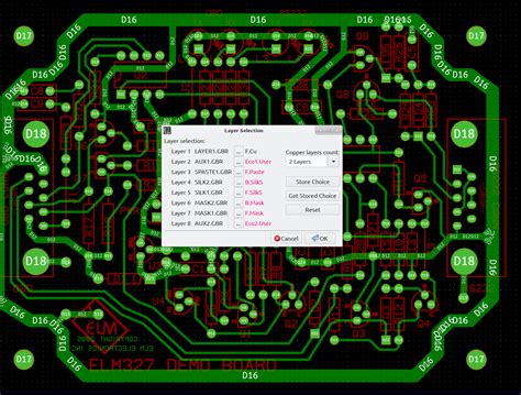
- Configure the Gerber file options:
- Select the layers to include in the Gerber files (e.g., copper layers, solder mask, silkscreen).
- Choose the appropriate Gerber file extension (e.g., .gbr, .gm1, .gts).
- Set the resolution and coordinate format (e.g., 4:4, mm).
- Click “Plot” to generate the Gerber files.
- In the same “Plot” dialog, switch to the “Drill Files” tab.
- Choose the “Excellon” format and set the output directory.
- Configure the drill file options (e.g., units, map file format).
- Click “Generate Drill File” to create the drill files.
After generating the Gerber and drill files, you will have a set of files that represent your PCB design, ready for manufacturing.

Verifying and Inspecting Gerber Files
Before sending your Gerber files to a PCB manufacturer, it is crucial to verify and inspect them for accuracy and completeness. Use the following tools and techniques to ensure the quality of your Gerber files:
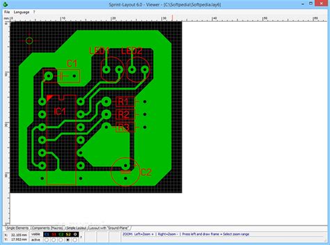
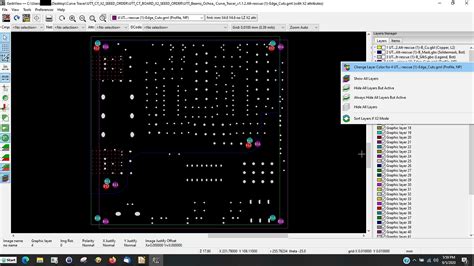
Gerber Viewer
Open your generated Gerber files in a Gerber viewer software, such as gerbv or ViewMate. A Gerber viewer allows you to visually inspect the PCB layers, check for any missing or incorrect features, and ensure that the files are properly aligned. Look for the following:
- Correct layer stackup and order
- Proper alignment of layers
- Complete and accurate copper features, pads, and traces
- Correct solder mask and Silkscreen placement
D-Code Check
In the PCB Editor, click on File -> Fabrication Outputs -> D-Code Info. Click on the button “D-Code Info”.
Review the generated D-Code report and ensure that all apertures used in the Gerber files are properly defined. D-Codes represent the shapes and sizes of pads, traces, and other features in the Gerber files. Verify that there are no missing or duplicate D-Codes.
Manufacturability Check
Many PCB manufacturers offer online tools or services to check the manufacturability of your Gerber files. These tools analyze your files for common manufacturing issues, such as minimum trace width, clearance, and drill sizes. Upload your Gerber files to the manufacturer’s website and review the feedback provided. Address any reported issues before proceeding with fabrication.
Common Issues and Troubleshooting
During the process of exporting KiCad PCB to Gerber files, you may encounter some common issues. Here are a few problems and their solutions:
Missing or Incorrect Layers
If certain layers are missing or incorrect in the generated Gerber files, double-check the layer selection in the “Plot” dialog. Ensure that all required layers are selected and properly named. Also, verify that the correct file extensions are used for each layer type.
Incorrect Board Outline
If the board outline is missing or incorrect in the Gerber files, review the “Edge.Cuts” layer in the PCB Editor. Make sure that the board outline is a closed shape and does not intersect with any components or features. Regenerate the Gerber files after making any necessary corrections.
Drill File Issues
If the drill files are missing or contain incorrect information, check the drill file settings in the “Plot” dialog. Verify that the correct drill file format (e.g., Excellon) is selected and that the drill units and map file format are properly configured. Also, ensure that all the required drill sizes are defined in the design.
Aperture or D-Code Errors
If you encounter aperture or D-Code errors during Gerber file generation or inspection, review the D-Code report and compare it with the apertures used in your design. Check for any missing or duplicate D-Codes and ensure that the aperture sizes match the design requirements. Update the aperture definitions in the PCB Editor if necessary.
Best Practices for Gerber File Generation
To ensure smooth and error-free Gerber file generation, follow these best practices:
- Keep your PCB design clean and organized, with proper layer stackup and naming conventions.
- Run Design Rule Checks (DRC) regularly during the design process to catch and fix issues early.
- Use a consistent grid size and unit system throughout your design.
- Provide clear and concise instructions to the PCB manufacturer, including any special requirements or considerations.
- Always verify and inspect your generated Gerber files before sending them for fabrication.
- Communicate with your PCB manufacturer if you have any questions or concerns regarding the Gerber files or fabrication process.
Frequently Asked Questions (FAQ)
- What are the essential layers to include in Gerber files?
-
The essential layers for Gerber files include:
- Top and bottom copper layers
- Top and bottom solder mask layers
- Top and bottom silkscreen layers
- Drill files (PTH and NPTH)
- Board outline (Edge.Cuts layer)
-
Can I generate Gerber files from a KiCad schematic?
-
No, Gerber files are generated from the PCB layout, not the schematic. You need to create a PCB layout based on your schematic and then export the Gerber files from the PCB Editor.
-
What is the recommended resolution and coordinate format for Gerber files?
-
The recommended resolution for Gerber files is 4:4 (0.1 micron) or higher. The coordinate format should be set to millimeters (mm) for consistency and compatibility with most PCB manufacturers.
-
How do I include multiple copper layers in the Gerber files?
-
In the “Plot” dialog, select all the required copper layers (e.g., F.Cu, B.Cu, In1.Cu, In2.Cu) in the layer list. Each copper layer will be exported as a separate Gerber file with the appropriate file extension.
-
What should I do if my PCB manufacturer reports issues with my Gerber files?
- If your PCB manufacturer reports issues with your Gerber files, first carefully review their feedback and try to understand the problem. Double-check your design and Gerber file settings, and make any necessary corrections. If you are unsure about how to resolve the issue, communicate with the manufacturer and seek their guidance. They may provide specific instructions or recommendations to fix the problem.
Conclusion
Exporting your KiCad PCB to Gerber files is a critical step in the PCB fabrication process. By following the steps outlined in this article, you can ensure that your Gerber files are accurate, complete, and ready for manufacturing. Remember to prepare your PCB design, generate the Gerber files with the appropriate settings, and verify and inspect them before sending them to your PCB manufacturer.
By adhering to best practices and addressing common issues, you can streamline the Gerber file generation process and avoid potential delays or problems during fabrication. Always communicate with your PCB manufacturer and seek their guidance if you have any questions or concerns.
With the knowledge gained from this article, you are now equipped to successfully export your KiCad PCB to Gerber files and bring your electronic designs to life.
No responses yet