Introduction to PCB Assembly
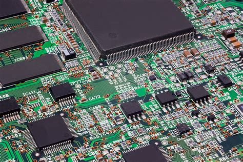
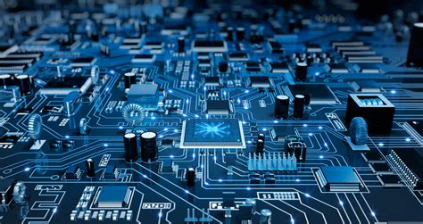
Printed Circuit Board (PCB) assembly is the process of attaching electronic components to a PCB to create a functional electronic device. The PCB serves as the foundation for the electronic circuit, providing both mechanical support and electrical connections between components. The assembly process involves several steps, each requiring precision and attention to detail to ensure the final product functions as intended.
In this article, we will delve into the various aspects of the PCB assembly process, including the types of PCB assembly, the steps involved, and the equipment and techniques used. By the end of this article, you will have a comprehensive understanding of how PCB assembly works and the factors that contribute to a successful assembly process.
Types of PCB Assembly
There are two main types of PCB assembly: Through-Hole Assembly (THA) and Surface Mount Assembly (SMA).
Through-Hole Assembly (THA)
Through-hole assembly involves inserting component leads through drilled holes in the PCB and soldering them to pads on the opposite side of the board. This assembly method is older and less frequently used today due to the advent of surface mount technology. However, it is still employed for certain components that require the mechanical strength and reliability provided by through-hole mounting.
Advantages of through-hole assembly include:
– Stronger mechanical bonds between components and the PCB
– Easier to replace or repair components
– Better suited for high-power applications
Disadvantages of through-hole assembly include:
– Larger component sizes and PCB footprints
– Increased drilling costs and time
– Limited component density compared to surface mount assembly
Surface Mount Assembly (SMA)
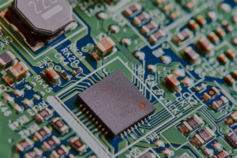
Surface mount assembly involves placing components directly onto pads on the surface of the PCB and soldering them in place. This assembly method has become the standard in modern electronics manufacturing due to its numerous advantages over through-hole assembly.
Advantages of surface mount assembly include:
– Smaller component sizes and PCB footprints
– Increased component density and functionality
– Faster assembly speeds and lower production costs
– Improved high-frequency performance
Disadvantages of surface mount assembly include:
– Requires specialized equipment and skilled operators
– More difficult to replace or repair components
– Sensitive to thermal stresses during soldering
PCB Assembly Process Steps
The PCB assembly process consists of several steps, each critical to ensuring a high-quality final product. These steps include:
- Solder Paste Application
- Component Placement
- Reflow Soldering
- Inspection and Quality Control
- Through-Hole Component Insertion (if applicable)
- Wave Soldering (if applicable)
- Final Inspection and Functional Testing
Step 1: Solder Paste Application
Solder paste, a mixture of tiny solder particles and flux, is applied to the PCB’s surface mount pads using a stencil or screen printing process. The stencil is a thin metal sheet with openings that correspond to the pads on the PCB. The solder paste is spread over the stencil, filling the openings and depositing the paste onto the pads when the stencil is removed.
Factors that affect the quality of solder paste application include:
– Stencil thickness and aperture size
– Solder paste viscosity and composition
– Printing parameters, such as squeegee pressure and speed
Step 2: Component Placement
Surface mount components are placed onto the solder paste-coated pads using a pick-and-place machine. These machines use vacuum nozzles or grippers to pick up components from feeders and place them accurately on the PCB. Modern pick-and-place machines can place thousands of components per hour with high precision.
Factors that affect component placement accuracy include:
– Machine calibration and maintenance
– Component packaging and orientation
– PCB design and pad layout
Step 3: Reflow Soldering
After component placement, the PCB undergoes reflow soldering, a process that melts the solder paste and forms a permanent electrical and mechanical connection between the components and the PCB. The PCB is passed through a reflow oven, which heats the board in a controlled manner, following a specific temperature profile.
The reflow soldering process consists of four main stages:
1. Preheat: The PCB is gradually heated to activate the flux and remove solvents.
2. Thermal soak: The temperature is maintained to ensure even heat distribution and flux activation.
3. Reflow: The temperature is raised above the solder’s melting point, allowing the solder to flow and form connections.
4. Cooling: The PCB is cooled to solidify the solder joints.
Factors that affect reflow soldering quality include:
– Reflow oven temperature profile
– Solder paste composition and quality
– Component and PCB thermal mass
Step 4: Inspection and Quality Control
After reflow soldering, the PCB undergoes visual and automated optical inspection (AOI) to identify any defects, such as bridging, Tombstoning, or insufficient solder. AOI systems use cameras and image processing algorithms to compare the assembled PCB to a reference image, highlighting any discrepancies.
Other inspection methods include:
– X-ray inspection for hidden solder joints
– In-circuit testing (ICT) for electrical continuity and component functionality
– Functional testing to verify overall product performance
Step 5: Through-Hole Component Insertion (if applicable)
If the PCB design includes through-hole components, they are inserted manually or using automated insertion machines after the surface mount components have been soldered. The through-hole components are placed into the drilled holes and secured in place for the next step.
Step 6: Wave Soldering (if applicable)
Wave soldering is used to solder through-hole components to the PCB. The board is passed over a molten solder wave, which contacts the component leads and PCB pads, creating a solder joint. A fluxing agent is applied to the board before wave soldering to clean and prepare the surfaces for soldering.
Factors that affect wave soldering quality include:
– Solder wave height and temperature
– Conveyor speed and angle
– Fluxing agent type and application
Step 7: Final Inspection and Functional Testing
After all soldering processes are complete, the PCB undergoes a final visual inspection and functional testing to ensure that it meets all performance and quality requirements. Any defective boards are reworked or scrapped, and the passing boards are packaged and shipped to the customer.

Equipment Used in PCB Assembly
Various equipment is used throughout the PCB assembly process to ensure accuracy, consistency, and efficiency. Some of the key equipment includes:
- Stencil Printer: Applies solder paste to the PCB pads
- Pick-and-Place Machine: Places surface mount components onto the PCB
- Reflow Oven: Melts the solder paste to form solder joints
- Automated Optical Inspection (AOI) Machine: Inspects the PCB for defects
- X-ray Inspection Machine: Inspects hidden solder joints
- In-Circuit Test (ICT) Machine: Tests for electrical continuity and component functionality
- Wave Soldering Machine: Solders through-hole components to the PCB
- Functional Test Equipment: Verifies overall product performance
Techniques Used in PCB Assembly
Several techniques are employed during the PCB assembly process to ensure high-quality results. These include:
- Electrostatic Discharge (ESD) Protection: Prevents damage to sensitive components from static electricity
- Moisture Sensitivity Level (MSL) Management: Controls the exposure of moisture-sensitive components to humidity
- Lean Manufacturing Principles: Minimizes waste and improves efficiency through continuous improvement
- Traceability and Documentation: Maintains records of materials, processes, and tests for quality assurance and troubleshooting
Frequently Asked Questions (FAQ)
1. What is the difference between through-hole and surface mount assembly?
Through-hole assembly involves inserting component leads through drilled holes in the PCB and soldering them to pads on the opposite side, while surface mount assembly involves placing components directly onto pads on the surface of the PCB and soldering them in place.
2. What are the main steps in the PCB assembly process?
The main steps in the PCB assembly process are solder paste application, component placement, reflow soldering, inspection and quality control, through-hole component insertion (if applicable), wave soldering (if applicable), and final inspection and functional testing.
3. What equipment is used in PCB assembly?
Key equipment used in PCB assembly includes stencil printers, pick-and-place machines, reflow ovens, automated optical inspection (AOI) machines, X-ray inspection machines, in-circuit test (ICT) machines, wave soldering machines, and functional test equipment.
4. What is the purpose of reflow soldering?
Reflow soldering melts the solder paste applied to the PCB pads, forming a permanent electrical and mechanical connection between the components and the PCB.
5. How is the quality of the assembled PCB ensured?
The quality of the assembled PCB is ensured through various inspection and testing methods, such as visual inspection, automated optical inspection (AOI), X-ray inspection, in-circuit testing (ICT), and functional testing. Additionally, proper process control, traceability, and documentation help maintain consistent quality throughout the assembly process.
Conclusion
PCB assembly is a complex process that requires precision, expertise, and specialized equipment to produce high-quality electronic devices. By understanding the different types of PCB assembly, the steps involved, and the equipment and techniques used, you can better appreciate the intricacies of this critical manufacturing process.
As technology continues to advance, PCB assembly processes will evolve to accommodate smaller, more complex designs and higher-density components. Staying up-to-date with the latest developments in PCB assembly will help ensure that your electronic products remain competitive and reliable in an ever-changing market.
No responses yet