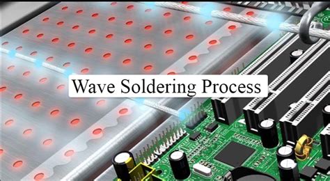
What is Wave Soldering?
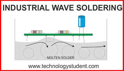
Wave soldering is a large-scale soldering process used for the mass production of printed circuit board (PCB) assemblies. It involves using a molten solder wave to efficiently solder electronic components to the PCB. The wave soldering machine consists of a conveyor system that carries the PCB over a pan of molten solder. As the board moves over the wave, the components on the bottom side of the PCB are soldered to the board.
Key Features of Wave Soldering:
- Automated process for high-volume production
- Suitable for through-hole components
- Molten solder wave used to solder components to PCB
- Conveyor system moves PCB over solder wave
- Flux applied before soldering to improve solder wetting
Advantages of Wave Soldering
1. High-Speed Production
One of the primary advantages of wave soldering is its ability to support high-speed production. The automated process allows for continuous soldering of PCBs, making it ideal for large-scale manufacturing. Wave soldering machines can process hundreds or even thousands of boards per hour, depending on the complexity of the assembly and the machine’s configuration.
2. Cost-Effectiveness
Wave soldering is a cost-effective solution for mass production of PCB assemblies. The automated nature of the process reduces labor costs and minimizes human error, resulting in lower overall production costs. Additionally, wave soldering uses less solder compared to other methods, such as selective soldering or hand soldering, which further contributes to cost savings.
3. Consistency and Reliability
The wave soldering process ensures consistent and reliable solder joints across the entire PCB. The molten solder wave provides uniform heat distribution and solder coverage, resulting in strong and durable connections between components and the board. This consistency is essential for producing high-quality electronics that meet industry standards and customer expectations.
4. Versatility
Wave soldering is versatile and can accommodate a wide range of component types and sizes. It is particularly well-suited for through-hole components, which are inserted into holes drilled in the PCB. The molten solder wave easily flows into these holes, creating strong solder joints. Wave soldering can also handle various board sizes and shapes, making it adaptable to different product designs.
5. Efficient Use of Flux
Flux is a chemical agent used in soldering to remove oxides and improve solder wetting. In wave soldering, flux is applied to the bottom side of the PCB before it enters the solder wave. The automated application of flux ensures an even distribution and minimizes waste compared to manual fluxing methods. Efficient use of flux helps improve the quality of solder joints and reduces the need for post-soldering cleaning.
Disadvantages of Wave Soldering
1. Limited Compatibility with Surface Mount Components
While wave soldering excels at soldering through-hole components, it has limitations when it comes to surface mount components (SMCs). SMCs are designed to be placed directly on the surface of the PCB, without the need for holes. Wave soldering can cause issues such as component displacement, bridging, or insufficient solder coverage for SMCs. As a result, alternative soldering methods, such as reflow soldering, are often used for SMCs.
2. Thermal Stress on Components
During wave soldering, the entire PCB is exposed to high temperatures, which can cause thermal stress on sensitive components. The sudden temperature change as the board enters and exits the molten solder wave can lead to component damage or failure. Proper component selection, placement, and thermal profiling are crucial to mitigate the risk of thermal stress.
3. Potential for Solder Defects
Although wave soldering provides consistent results, it is not immune to solder defects. Common defects include:
- Solder bridges: Unintended connections between adjacent pins or pads
- Incomplete solder joints: Insufficient solder coverage or poor wetting
- Solder balls: Small spheres of solder that can cause short circuits
- Icicles: Excessive solder buildup on component leads
These defects can be caused by various factors, such as improper flux application, incorrect solder temperature, or inadequate board cleaning. Implementing proper process controls and regular maintenance of the wave soldering equipment can help minimize the occurrence of solder defects.
4. Limited Design Flexibility
Wave soldering imposes certain design constraints on PCBs. The process requires adequate spacing between components to prevent shadowing effects and ensure proper solder flow. Additionally, the orientation and placement of components must consider the direction of the solder wave to avoid turbulence and ensure even solder distribution. These design considerations may limit the flexibility in component placement and board layout compared to other soldering methods.
5. Environmental Concerns
Wave soldering involves the use of lead-based solder alloys, which can have environmental and health implications. Lead is a toxic substance, and its use in electronics is regulated by various directives, such as the Restriction of Hazardous Substances (RoHS) directive. Compliance with these regulations may require the use of lead-free solder alloys, which can present challenges in terms of process control and joint reliability.

Comparing Wave Soldering with Other Soldering Methods
To better understand the advantages and disadvantages of wave soldering, it is helpful to compare it with other common soldering methods used in PCB assembly.
Wave Soldering vs. Reflow Soldering
Reflow soldering is a process used for soldering surface mount components (SMCs) to PCBs. It involves applying solder paste to the pads on the board, placing the components, and then heating the entire assembly in a reflow oven to melt the solder and form the joints.
| Feature | Wave Soldering | Reflow Soldering |
|---|---|---|
| Component Compatibility | Primarily through-hole components | Surface mount components |
| Process Speed | High-speed, continuous process | Batch process, limited by oven capacity |
| Solder Joint Consistency | Uniform solder wave ensures consistency | Depends on solder paste application and reflow profile |
| Design Flexibility | Limited by component spacing and orientation | Higher flexibility in component placement |
| Environmental Impact | Typically uses lead-based solder | Can use lead-free solder paste |
Wave Soldering vs. Selective Soldering
Selective soldering is a targeted soldering process that uses a localized solder wave or jet to solder specific components or areas on a PCB. It offers more flexibility than wave soldering and is often used for mixed-technology boards that contain both through-hole and surface mount components.
| Feature | Wave Soldering | Selective Soldering |
|---|---|---|
| Process Scope | Solders all components on the bottom side of the PCB | Solders specific components or areas |
| Speed and Throughput | High-speed, continuous process | Slower, targeted process |
| Component Compatibility | Primarily through-hole components | Both through-hole and surface mount components |
| Flexibility | Limited by component spacing and orientation | Highly flexible, can solder complex layouts |
| Investment Cost | Lower initial investment | Higher equipment cost due to specialized machines |
Wave Soldering vs. Hand Soldering
Hand soldering is a manual soldering process that involves using a soldering iron to solder individual components to the PCB. It is often used for prototyping, rework, or low-volume production.
| Feature | Wave Soldering | Hand Soldering |
|---|---|---|
| Production Volume | High-volume, automated process | Low-volume, manual process |
| Consistency | Uniform solder wave ensures consistency | Depends on operator skill and technique |
| Speed | High-speed, continuous process | Slow, labor-intensive process |
| Flexibility | Limited by component spacing and orientation | Highly flexible, can solder any component type |
| Cost | Cost-effective for large-scale production | Higher labor costs, suitable for low-volume or rework |
Frequently Asked Questions (FAQ)
1. What types of components are best suited for wave soldering?
Wave soldering is primarily used for through-hole components, which have leads that are inserted into holes drilled in the PCB. It is less suitable for surface mount components (SMCs) due to the risk of component displacement or insufficient solder coverage.
2. Can wave soldering be used for double-sided PCBs?
Yes, wave soldering can be used for double-sided PCBs, but it requires special considerations. The components on the top side of the board must be glued or mechanically secured to prevent them from falling off during the soldering process. Additionally, a selective soldering process may be used to solder components on the top side after the bottom side has been wave soldered.
3. What are the key factors to consider when setting up a wave soldering process?
The key factors to consider when setting up a wave soldering process include:
- Solder alloy selection (lead-based or lead-free)
- Solder temperature and wave height
- Flux type and application method
- Conveyor speed and board orientation
- Preheat temperature and duration
- PCB design and component placement
Proper optimization of these factors is crucial for achieving high-quality solder joints and minimizing defects.
4. How can solder defects be minimized in wave soldering?
Solder defects in wave soldering can be minimized by implementing the following measures:
- Ensuring proper PCB design and component placement
- Optimizing the solder wave parameters (temperature, height, etc.)
- Using appropriate flux and applying it evenly
- Maintaining the cleanliness of the PCB and the soldering equipment
- Implementing process controls and regular quality inspections
- Providing adequate training to operators and technicians
5. Is wave soldering environmentally friendly?
Traditional wave soldering uses lead-based solder alloys, which can have negative environmental and health impacts. However, many companies have transitioned to using lead-free solder alloys to comply with environmental regulations such as the Restriction of Hazardous Substances (RoHS) directive. Lead-free wave soldering presents its own challenges, such as higher processing temperatures and different wetting characteristics, but it offers a more environmentally friendly alternative.
Conclusion
Wave soldering is a widely used soldering process in the electronics industry, offering numerous advantages for the mass production of PCB assemblies. Its high-speed, cost-effectiveness, and consistency make it an attractive option for manufacturers. However, it is essential to consider the limitations and potential disadvantages, such as limited compatibility with surface mount components and the risk of thermal stress on sensitive components.
When deciding whether to use wave soldering for a particular project, it is crucial to evaluate the specific requirements, such as component types, board design, production volume, and environmental considerations. Understanding the advantages and disadvantages of wave soldering and comparing it with other soldering methods can help make informed decisions and optimize the manufacturing process.
By implementing proper process controls, regular maintenance, and continuous improvement initiatives, manufacturers can leverage the benefits of wave soldering while minimizing the occurrence of defects and ensuring high-quality soldered assemblies. As technology advances and environmental regulations evolve, the wave soldering process will likely continue to adapt and remain a valuable tool in the electronics manufacturing industry.
No responses yet