What is a Circuit Board?
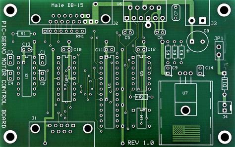
A circuit board, also known as a printed circuit board (PCB), is a flat board made of insulating material with conductive tracks, pads, and other features etched from copper sheets laminated onto a non-conductive substrate. It is used to mechanically support and electrically connect electronic components using conductive pathways, tracks, or signal traces etched from copper sheets laminated onto a non-conductive substrate.
Why is Circuit Board Design Important?
Circuit board design is a critical aspect of electronic product development. It involves the creation of a custom PCB that is optimized for a specific application. A well-designed circuit board can improve the performance, reliability, and manufacturability of an electronic product, while a poorly designed board can lead to issues such as signal integrity problems, electromagnetic interference (EMI), and manufacturing defects.
Step 1: Define Your Requirements
Before you start designing your circuit board, it’s important to define your requirements. This includes identifying the purpose of your board, the components you’ll be using, and any specific design constraints you may have. Some key factors to consider include:
- Board size and shape
- Number and type of components
- Power requirements
- Signal integrity and EMI considerations
- Environmental factors (temperature, humidity, etc.)

Step 2: Choose Your Design Software
There are many different software tools available for circuit board design, ranging from free open-source programs to high-end commercial solutions. Some popular options include:
- KiCad (free and open-source)
- Eagle (free for non-commercial use)
- Altium Designer (commercial)
- OrCAD (commercial)
When choosing your design software, consider factors such as ease of use, feature set, and compatibility with your other tools and workflows.
Step 3: Create Your Schematic
The first step in designing your circuit board is to create a schematic diagram. This is a graphical representation of your circuit that shows how the components are connected together. Your schematic should include:
- All components and their values
- Power and ground connections
- Input and output signals
- Any special requirements (e.g. high-speed signals, sensitive analog circuits)
When creating your schematic, it’s important to follow best practices such as using consistent naming conventions, grouping related components together, and adding clear labels and annotations.
Step 4: Select Your Components
Once you have your schematic, the next step is to select the specific components you’ll be using. This involves choosing parts that meet your requirements for performance, cost, and availability. Some key factors to consider include:
- Voltage and current ratings
- Package type and size
- Tolerance and accuracy
- Thermal characteristics
- Availability and lead time
When selecting components, it’s also important to consider factors such as obsolescence risk and compliance with any relevant standards or regulations.
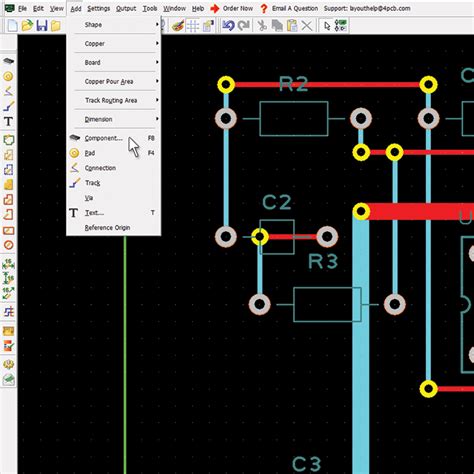
Step 5: Create Your PCB Layout
With your schematic and components selected, you can now move on to creating your PCB layout. This involves arranging your components on the board and routing the connections between them. Some key considerations for PCB layout include:
- Component placement and orientation
- Signal integrity and EMI
- Thermal management
- Manufacturing constraints (e.g. minimum trace width and spacing)
When creating your PCB layout, it’s important to follow best practices such as minimizing the length of high-speed traces, avoiding sharp corners and 90-degree angles, and using ground planes and shielding to minimize EMI.
Step 6: Perform Design Rule Checks
Before finalizing your PCB layout, it’s important to perform design rule checks (DRCs) to ensure that your design meets all the necessary requirements. This involves checking for issues such as:
- Minimum trace width and spacing violations
- Unconnected or shorted nets
- Overlapping components or traces
- Incorrect hole sizes or pad shapes
Most PCB design software includes built-in DRC tools that can automatically check your design against a set of predefined rules. It’s important to run these checks regularly throughout the design process to catch any issues early on.
Step 7: Generate Manufacturing Files
Once your PCB layout is finalized and passes all DRCs, you can generate the necessary manufacturing files. These typically include:
- Gerber files (for the PCB layers)
- Drill files (for the holes and vias)
- BOM (Bill of Materials) and assembly drawings
It’s important to work closely with your PCB manufacturer to ensure that your files are in the correct format and meet their specific requirements.
Step 8: Review and Verify Your Design
Before sending your design off for manufacturing, it’s important to review and verify it thoroughly. This involves checking for any errors or omissions, as well as ensuring that your design meets all the necessary requirements for performance, reliability, and manufacturability. Some key steps in the review process include:
- Visual inspection of the PCB layout
- Electrical and Signal integrity simulations
- Mechanical and thermal analysis
- Manufacturing and assembly feasibility checks
It’s also a good idea to have your design reviewed by other engineers or experts to get a fresh perspective and catch any issues you may have missed.
Step 9: Send for Manufacturing
Once your design is finalized and verified, you can send it off for manufacturing. This involves working with a PCB fabrication and assembly company to produce your boards. Some key steps in the manufacturing process include:
- Generating a quote and placing an order
- Providing your manufacturing files and any necessary documentation
- Communicating any special requirements or instructions
- Reviewing and approving prototypes or samples
- Arranging for shipping and delivery
It’s important to work closely with your manufacturing partner throughout the process to ensure that your boards are produced to your specifications and meet all the necessary quality and reliability standards.
Step 10: Test and Validate Your Design
Once you receive your manufactured boards, the final step is to test and validate your design. This involves powering up your boards and verifying that they function as intended. Some key steps in the testing process include:
- Visual inspection for any manufacturing defects
- Functional testing of all components and features
- Performance and reliability testing under different conditions
- Compliance testing for any relevant standards or regulations
If any issues are found during testing, it may be necessary to go back and modify your design or manufacturing process to address them. It’s important to document all testing results and any necessary changes for future reference.
FAQs
- What is the difference between a schematic and a PCB layout?
-
A schematic is a graphical representation of the electrical connections in a circuit, while a PCB layout is a physical representation of how the components are arranged on the board.
-
What are some common PCB manufacturing methods?
-
Some common PCB manufacturing methods include etching, milling, and photolithography. The choice of method depends on factors such as the complexity of the design, the required level of precision, and the production volume.
-
What is the purpose of design rule checks (DRCs)?
-
DRCs are used to ensure that a PCB design meets all the necessary requirements for manufacturability, reliability, and performance. They help catch issues such as minimum trace width and spacing violations, unconnected or shorted nets, and overlapping components or traces.
-
What are some common file formats used in PCB manufacturing?
-
Some common file formats used in PCB manufacturing include Gerber files (for the PCB layers), drill files (for the holes and vias), and BOM (bill of materials) and assembly drawings. The specific formats used may vary depending on the manufacturer and the design software being used.
-
How can I ensure the reliability and quality of my manufactured PCBs?
- To ensure the reliability and quality of your manufactured PCBs, it’s important to work closely with a reputable PCB fabrication and assembly company, provide clear and accurate manufacturing files and documentation, and thoroughly test and validate your design before and after manufacturing. It’s also a good idea to establish quality control processes and standards, and to regularly communicate with your manufacturing partner to address any issues or concerns.
| Step | Description |
|---|---|
| 1 | Define Your Requirements |
| 2 | Choose Your Design Software |
| 3 | Create Your Schematic |
| 4 | Select Your Components |
| 5 | Create Your PCB Layout |
| 6 | Perform Design Rule Checks |
| 7 | Generate Manufacturing Files |
| 8 | Review and Verify Your Design |
| 9 | Send for Manufacturing |
| 10 | Test and Validate Your Design |
By following these 10 steps and working closely with your manufacturing partner, you can design and produce high-quality, reliable circuit boards that meet your specific requirements and exceed your expectations. Remember to stay organized, communicate clearly, and always prioritize quality and attention to detail throughout the design and manufacturing process.
No responses yet