Understanding PCB Thickness and Its Importance
Printed Circuit Boards (PCBs) are essential components in modern electronics, providing a platform for mounting and interconnecting electronic components. One of the critical factors to consider when designing or selecting a PCB is its thickness. PCB thickness plays a vital role in the overall performance, durability, and functionality of the circuit board. In this article, we will explore the various aspects of PCB thickness and provide guidance on how to choose the right thickness for your specific application.
What is PCB Thickness?
PCB thickness refers to the distance between the top and bottom surfaces of the circuit board. It is typically measured in millimeters (mm) or mils (thousandths of an inch). The thickness of a PCB is determined by the number of copper layers, the thickness of each layer, and the thickness of the insulating substrate material.
Why is PCB Thickness Important?
The thickness of a PCB has a significant impact on several aspects of its performance and functionality:
-
Mechanical Strength: Thicker PCBs offer greater mechanical strength and rigidity, making them more resistant to bending, twisting, and vibrations. This is particularly important for applications that require high reliability and durability.
-
Thermal Management: Thicker PCBs have better thermal conductivity, allowing for more efficient heat dissipation from electronic components. This helps prevent overheating and extends the lifespan of the components.
-
Electrical Performance: PCB thickness can affect the electrical characteristics of the circuit board, such as impedance, capacitance, and inductance. Proper thickness selection is crucial for maintaining signal integrity and minimizing electromagnetic interference (EMI).
-
Manufacturing Constraints: The choice of PCB thickness is also influenced by manufacturing capabilities and constraints. Thinner PCBs are generally more challenging to manufacture and may require specialized equipment and processes.
Standard PCB Thicknesses and Their Applications
PCBs are available in various standard thicknesses to cater to different application requirements. Here are some common PCB thicknesses and their typical applications:
| PCB Thickness (mm) | PCB Thickness (mils) | Typical Applications |
|---|---|---|
| 0.4 | 15.7 | Flexible PCBs, wearable electronics |
| 0.6 | 23.6 | Mobile devices, consumer electronics |
| 0.8 | 31.5 | General-purpose PCBs, low-power applications |
| 1.0 | 39.4 | Automotive electronics, industrial control systems |
| 1.2 | 47.2 | High-power applications, military and aerospace |
| 1.6 | 63.0 | Multilayer PCBs, complex designs |
| 2.0 | 78.7 | Backplanes, high-speed applications |
Thin PCBs (0.4mm – 0.8mm)
Thin PCBs, ranging from 0.4mm to 0.8mm, are commonly used in applications that require flexibility, lightweight, and compact form factors. These PCBs are often found in mobile devices, wearable electronics, and consumer products. Thin PCBs offer several advantages, such as reduced weight, improved flexibility, and better heat dissipation due to their high surface area-to-volume ratio.
However, thin PCBs also have some limitations. They are more susceptible to mechanical stress and may require additional support or reinforcement to prevent damage. Additionally, thin PCBs may have lower current carrying capacity and may be more challenging to manufacture compared to thicker PCBs.
Standard PCBs (1.0mm – 1.6mm)
Standard PCB thicknesses, ranging from 1.0mm to 1.6mm, are widely used in a variety of applications, including automotive electronics, industrial control systems, and general-purpose PCBs. These thicknesses provide a good balance between mechanical strength, thermal management, and electrical performance.
PCBs with a thickness of 1.0mm to 1.6mm offer sufficient rigidity and durability for most applications. They can accommodate a higher number of copper layers and are suitable for designs with moderate to high component density. These PCBs are also easier to manufacture compared to thinner PCBs, making them a cost-effective choice for many projects.
Thick PCBs (2.0mm and above)
Thick PCBs, with a thickness of 2.0mm or more, are used in applications that demand exceptional mechanical strength, high power handling capability, and superior thermal management. These PCBs are commonly found in backplanes, high-speed applications, and military and aerospace systems.
Thick PCBs offer several advantages over thinner PCBs. They provide excellent mechanical stability and can withstand harsh environmental conditions, such as extreme temperatures, vibrations, and shocks. Thick PCBs also have better thermal conductivity, allowing for efficient heat dissipation from power-hungry components.
However, thick PCBs may have some drawbacks. They are heavier and bulkier compared to thinner PCBs, which may not be suitable for applications with strict space constraints. Additionally, thick PCBs may require specialized manufacturing processes and may be more expensive to produce.

Factors to Consider When Choosing PCB Thickness
When selecting the appropriate PCB thickness for your application, there are several factors to consider. These factors will help you determine the optimal thickness that meets your design requirements, manufacturing constraints, and cost considerations.
1. Application Requirements
The first and foremost factor to consider is the specific requirements of your application. Different applications have varying demands in terms of mechanical strength, thermal management, and electrical performance. For example:
- Mobile devices and wearable electronics often require thin and flexible PCBs to fit into compact form factors and provide comfortable user experience.
- Automotive electronics and industrial control systems may require thicker PCBs to withstand harsh environmental conditions and ensure long-term reliability.
- High-speed applications, such as telecommunications and data centers, may require specific PCB thicknesses to maintain signal integrity and minimize signal loss.
Consider the operating environment, expected lifespan, and performance requirements of your application when selecting the PCB thickness.
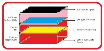
2. Number of Copper Layers
The number of copper layers in a PCB directly affects its thickness. Each additional copper layer adds to the overall thickness of the board. Therefore, the more layers your design requires, the thicker the PCB will be.
When choosing the number of layers and the resulting PCB thickness, consider the complexity of your circuit design, the routing requirements, and the signal integrity needs. Multilayer PCBs offer more routing flexibility and can accommodate higher component density compared to single or double-layer PCBs.
3. Component Placement and Height
The placement and height of components on the PCB also influence the choice of thickness. If your design includes tall components or requires components to be mounted on both sides of the board, you may need to opt for a thicker PCB to provide sufficient clearance and prevent component interference.
Additionally, consider the soldering process and the required standoff height for components. Thicker PCBs provide more space for proper soldering and can accommodate larger components with higher standoff heights.
4. Manufacturing Capabilities and Constraints
The manufacturing capabilities of your PCB fabricator and the constraints of the manufacturing process also play a role in determining the appropriate PCB thickness. Some PCB manufacturers may have limitations on the minimum and maximum thicknesses they can produce.
Thinner PCBs often require more advanced manufacturing techniques and tighter tolerances, which can increase production costs and lead times. On the other hand, thicker PCBs may require specialized drilling and plating processes, which can also impact manufacturing feasibility and cost.
Consult with your PCB manufacturer to understand their capabilities and constraints, and choose a PCB thickness that aligns with their manufacturing processes to ensure cost-effective and reliable production.
5. Cost Considerations
PCB thickness also has an impact on the overall cost of your project. In general, thinner PCBs are more expensive to manufacture compared to thicker PCBs due to the specialized processes and tighter tolerances required.
However, the cost of the PCB should be balanced against the overall system cost and the specific requirements of your application. In some cases, investing in a thicker PCB may result in better performance, reliability, and longevity, which can offset the initial higher cost in the long run.
Consider the total cost of ownership, including manufacturing, assembly, and potential rework or replacement costs, when selecting the PCB thickness. Strike a balance between cost and performance to ensure the best value for your project.

PCB Thickness Selection Process
Now that we have explored the various factors to consider when choosing PCB thickness, let’s outline a step-by-step process to help you make an informed decision.
-
Define application requirements: Start by clearly defining the requirements of your application, including the operating environment, expected lifespan, performance targets, and any specific mechanical or electrical constraints.
-
Determine the number of layers: Based on your circuit complexity and routing requirements, determine the number of copper layers needed for your PCB design. Keep in mind that more layers will result in a thicker PCB.
-
Consider component placement and height: Evaluate the placement and height of components on your PCB. Identify any tall components or special mounting requirements that may affect the choice of PCB thickness.
-
Consult with PCB manufacturer: Engage with your PCB manufacturer to discuss their capabilities, constraints, and recommendations for PCB thickness. They can provide valuable insights based on their experience and expertise.
-
Evaluate cost implications: Assess the cost implications of different PCB thicknesses, considering manufacturing costs, assembly costs, and potential long-term savings in terms of reliability and performance.
-
Make an informed decision: Based on the above factors, make an informed decision on the optimal PCB thickness that meets your application requirements, manufacturing constraints, and cost considerations.
-
Prototype and test: Once you have selected the PCB thickness, create prototypes and conduct thorough testing to validate your choice. Monitor the performance, reliability, and durability of the PCB under real-world conditions.
-
Iterate and optimize: Based on the results of prototyping and testing, iterate and optimize your PCB design if necessary. Fine-tune the thickness and other design parameters to achieve the best possible outcome for your application.
By following this process and carefully considering the relevant factors, you can select the most suitable PCB thickness for your specific application, ensuring optimal performance, reliability, and cost-effectiveness.

Frequently Asked Questions (FAQ)
-
What is the most common PCB thickness?
The most common PCB thickness is 1.6mm (63 mils). This thickness is widely used for general-purpose PCBs and offers a good balance between mechanical strength, thermal management, and electrical performance. -
Can I use a thinner PCB to save cost?
While using a thinner PCB may seem like a cost-saving option, it is essential to consider the overall impact on your application. Thinner PCBs may be more challenging to manufacture and may have limitations in terms of mechanical strength and current carrying capacity. It is crucial to strike a balance between cost and performance to ensure the long-term reliability and functionality of your product. -
How does PCB thickness affect signal integrity?
PCB thickness can have an impact on signal integrity, especially in high-speed applications. Thinner PCBs may be more susceptible to signal loss and crosstalk due to the closer proximity of copper layers. Thicker PCBs, on the other hand, can provide better signal integrity by allowing for wider trace widths and increased spacing between layers. The choice of PCB thickness should be based on the specific signal integrity requirements of your application. -
Can I mix different PCB thicknesses in the same design?
Yes, it is possible to use different PCB thicknesses within the same design, known as a “rigid-flex” or “multi-thickness” PCB. This approach is commonly used when certain sections of the PCB require different mechanical or electrical properties. For example, you can have a thicker section for power components and a thinner section for flexible connections. However, designing and manufacturing multi-thickness PCBs can be more complex and costly compared to standard single-thickness PCBs. -
How do I determine the appropriate PCB thickness for my application?
To determine the appropriate PCB thickness for your application, consider the following factors: - Application requirements: Assess the mechanical, thermal, and electrical demands of your application.
- Number of layers: Determine the number of copper layers needed based on your circuit complexity and routing requirements.
- Component placement and height: Consider the placement and height of components on the PCB.
- Manufacturing capabilities and constraints: Consult with your PCB manufacturer to understand their capabilities and constraints.
- Cost considerations: Evaluate the cost implications of different PCB thicknesses, considering manufacturing, assembly, and long-term costs.
By carefully evaluating these factors and consulting with PCB experts, you can make an informed decision on the most suitable PCB thickness for your specific application.
Conclusion
Choosing the right PCB thickness is a critical aspect of PCB design and manufacturing. The thickness of a PCB has a significant impact on its mechanical strength, thermal management, electrical performance, and manufacturing feasibility. By understanding the various factors that influence PCB thickness and following a systematic selection process, you can ensure that your PCB meets the specific requirements of your application while optimizing cost and reliability.
When selecting PCB thickness, consider the application requirements, the number of copper layers, component placement and height, manufacturing capabilities and constraints, and cost implications. Engage with your PCB manufacturer to leverage their expertise and ensure that your chosen thickness aligns with their manufacturing processes.
Remember that the optimal PCB thickness may vary depending on the unique demands of your application. It is essential to strike a balance between performance, reliability, and cost to achieve the best possible outcome for your project.
By carefully evaluating your options and making informed decisions, you can select the most suitable PCB thickness that meets your design goals, ensures reliable performance, and maximizes the success of your electronic product.
No responses yet