Understanding Soldering Temperatures and PCB Thermal Stress
When it comes to assembling electronic components on a printed circuit board (PCB), soldering is a crucial process that involves heating the PCB and components to a specific temperature to create reliable electrical connections. However, exposing a PCB to high temperatures repeatedly can lead to thermal stress, which may affect the board’s integrity and functionality. In this article, we will discuss how often you can raise a PCB to lead-free soldering temperatures without compromising its quality.
What is Lead-free Soldering?
Lead-free soldering is a process that uses solder alloys without lead, typically consisting of tin, silver, and copper (SAC alloys). This shift towards lead-free soldering was driven by environmental and health concerns associated with lead exposure. The most common lead-free solder alloy is SAC305, which contains 96.5% tin, 3% silver, and 0.5% copper.
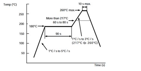
Lead-free Soldering Temperature Profile
To ensure proper solder joint formation and minimize thermal stress on the PCB, it is essential to follow a specific temperature profile during the lead-free soldering process. A typical lead-free soldering temperature profile consists of four stages:
- Preheat: The PCB is gradually heated to a temperature of 150-180°C to minimize thermal shock and activate the flux.
- Thermal Soak: The PCB is maintained at a stable temperature of 180-200°C for 60-120 seconds to ensure even heat distribution and further activate the flux.
- Reflow: The temperature is rapidly increased to the peak temperature of 235-260°C, depending on the solder alloy used, and held for 20-40 seconds to allow the solder to melt and form reliable connections.
- Cooling: The PCB is allowed to cool down gradually to room temperature to prevent thermal shock and ensure proper solder joint solidification.
| Stage | Temperature Range (°C) | Duration (seconds) |
|---|---|---|
| Preheat | 150-180 | 60-120 |
| Thermal Soak | 180-200 | 60-120 |
| Reflow | 235-260 | 20-40 |
| Cooling | Room temperature | – |
Thermal Stress on PCBs During Soldering
Exposing a PCB to high temperatures during the soldering process can cause thermal stress, which may lead to various issues, such as:
- Warping: Uneven heating or cooling can cause the PCB to warp, affecting its flatness and potentially leading to component misalignment or solder joint failures.
- Delamination: Repeated thermal stress can cause the layers of the PCB to separate, compromising its structural integrity and electrical performance.
- Copper Annealing: Exposure to high temperatures can cause the copper traces on the PCB to soften and become more susceptible to damage or deformation.
- Component Degradation: Some electronic components, particularly those with plastic packages, may degrade or become damaged when exposed to high temperatures repeatedly.
Factors Affecting PCB Thermal Stress Tolerance
Several factors influence a PCB’s ability to withstand repeated exposure to lead-free soldering temperatures:
- PCB Material: The choice of PCB material, such as FR-4, high-Tg FR-4, or polyimide, can significantly impact its thermal stress tolerance. High-Tg materials have better thermal stability and are more suitable for applications requiring multiple soldering cycles.
- PCB Thickness: Thicker PCBs are generally more resistant to warping and delamination caused by thermal stress compared to thinner ones.
- Copper Weight: The thickness of the copper traces on the PCB can affect its thermal stress tolerance. Thicker copper traces are more resilient to thermal stress and less likely to suffer from annealing effects.
- Component Selection: Choosing components with higher temperature ratings and more robust packages can help minimize the risk of component degradation during repeated soldering cycles.
Minimizing Thermal Stress During Soldering
To minimize the thermal stress on a PCB during lead-free soldering and increase its tolerance to repeated soldering cycles, consider the following best practices:
- Follow the Recommended Temperature Profile: Adhere to the recommended lead-free soldering temperature profile to ensure proper solder joint formation while minimizing thermal stress on the PCB and components.
- Use Appropriate Solder Alloys: Select lead-free solder alloys with lower melting points, such as SAC305, to reduce the peak temperature required during the reflow stage.
- Optimize PCB Design: Design the PCB with thermal stress in mind, incorporating features such as uniform Copper Distribution, proper component placement, and adequate spacing between components to promote even heat distribution and minimize localized thermal stress.
- Implement Controlled Cooling: Ensure a controlled and gradual cooling process after soldering to prevent thermal shock and minimize the risk of PCB warping or component damage.
- Use Thermal Relief Pads: Incorporate thermal relief pads for large components or heat-sensitive areas to help dissipate heat more efficiently and reduce thermal stress on the PCB.
How Often Can You Safely Raise a PCB to Lead-free Soldering Temperatures?
The number of times a PCB can be safely exposed to lead-free soldering temperatures depends on various factors, such as the PCB material, thickness, copper weight, and component selection. However, as a general guideline:
- Standard FR-4 PCBs: Can typically withstand 3-5 soldering cycles without significant degradation in performance or reliability.
- High-Tg FR-4 PCBs: Can withstand 5-7 soldering cycles due to their enhanced thermal stability.
- Polyimide PCBs: Can withstand 10 or more soldering cycles, making them suitable for applications requiring frequent rework or component replacement.
It is important to note that these figures are approximate and may vary depending on the specific PCB design, components used, and soldering process employed. Always consult with your PCB Manufacturer and assembly provider to determine the optimal number of soldering cycles for your specific application.
Frequently Asked Questions (FAQ)
-
Q: What is the main difference between lead-free and leaded soldering?
A: Lead-free soldering uses solder alloys without lead, typically consisting of tin, silver, and copper (SAC alloys), while leaded soldering uses solder alloys containing lead, such as tin-lead (SnPb) alloys. Lead-free soldering requires higher peak temperatures compared to leaded soldering. -
Q: Can I use the same temperature profile for all lead-free solder alloys?
A: No, different lead-free solder alloys may have slightly different melting points and require adjustments to the temperature profile. Always refer to the solder alloy manufacturer’s recommendations and consult with your assembly provider to determine the appropriate temperature profile for your specific solder alloy. -
Q: How can I tell if my PCB has suffered from thermal stress?
A: Signs of thermal stress on a PCB include warping, delamination, discoloration, or component damage. Electrical performance issues, such as intermittent connections or signal integrity problems, may also indicate thermal stress-related damage. Visual inspection and functional testing can help identify thermal stress-related issues. -
Q: Can I mix lead-free and leaded components on the same PCB?
A: While it is possible to mix lead-free and leaded components on the same PCB, it is generally not recommended. Mixing lead-free and leaded soldering processes can result in reliability issues due to the different melting points and thermal requirements of the solder alloys. If mixing is necessary, consult with your assembly provider to develop a compatible soldering process. -
Q: How can I extend the life of my PCB when exposed to repeated soldering cycles?
A: To extend the life of your PCB when exposed to repeated soldering cycles, consider using high-Tg or polyimide materials, increasing the PCB thickness and copper weight, selecting components with higher temperature ratings, optimizing the PCB design for thermal management, and implementing controlled cooling processes. Additionally, follow best practices for lead-free soldering and minimize the number of soldering cycles whenever possible.

Conclusion
Raising a PCB to lead-free soldering temperatures is an essential part of the Electronic Assembly process, but it can also expose the PCB to thermal stress. The number of times a PCB can safely withstand lead-free soldering temperatures depends on various factors, such as the PCB material, thickness, copper weight, and component selection. As a general guideline, standard FR-4 PCBs can typically withstand 3-5 soldering cycles, while high-Tg FR-4 and polyimide PCBs can withstand more cycles due to their enhanced thermal stability.
To minimize thermal stress and extend the life of your PCB, follow best practices for lead-free soldering, such as adhering to the recommended temperature profile, using appropriate solder alloys, optimizing PCB design, implementing controlled cooling, and using thermal relief pads. By understanding the factors affecting PCB thermal stress tolerance and taking appropriate measures, you can ensure reliable and long-lasting electronic assemblies that can withstand multiple soldering cycles.

No responses yet