What is Double-Sided SMT?
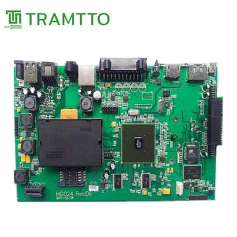
Double-sided SMT (Surface Mount Technology) is a process of assembling electronic components on both sides of a printed circuit board (PCB). This technique has become increasingly popular in the electronics industry due to its ability to maximize space utilization and improve the overall functionality of the PCB. In this article, we will explore the intricacies of double-sided SMT assembly and how it works.
Advantages of Double-Sided SMT
- Space Savings: By utilizing both sides of the PCB, double-sided SMT allows for a more compact design, reducing the overall size of the electronic device.
- Increased Functionality: With components placed on both sides of the PCB, more complex circuits can be created, enabling enhanced functionality and performance.
- Cost-Effective: Double-sided SMT assembly can lead to cost savings by reducing the number of PCBs required for a given design and minimizing the use of connectors and wires.
The Double-Sided SMT Assembly Process
The double-sided SMT assembly process involves several steps, each of which is critical to ensuring a high-quality end product. Let’s take a closer look at each step:
Step 1: PCB Design and Preparation
The first step in double-sided SMT assembly is designing the PCB layout using specialized software. The design must consider the placement of components on both sides of the board, as well as the routing of traces and vias to ensure proper electrical connections. Once the design is finalized, the PCB is manufactured and prepared for the assembly process.
Step 2: Solder Paste Application
Solder paste, a mixture of tiny solder particles suspended in a flux medium, is applied to the PCB pads using a stencil printing process. The stencil is a thin metal sheet with openings that correspond to the PCB pads. The solder paste is spread over the stencil, filling the openings and depositing the paste onto the pads.
Step 3: Component Placement
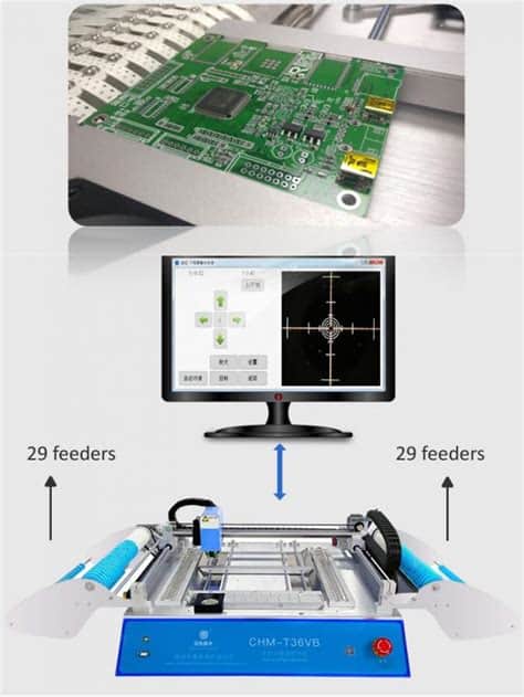
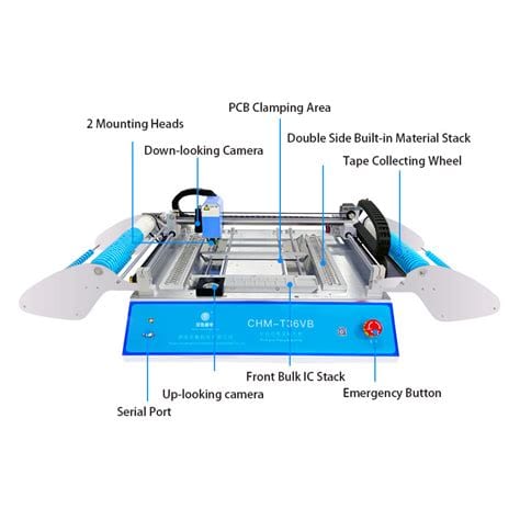
After the solder paste application, the electronic components are placed onto the PCB using a pick-and-place machine. This automated equipment uses vacuum nozzles to pick up components from reels or trays and precisely place them on the PCB pads. The machine is programmed with the component placement data from the PCB design file to ensure accurate positioning.
Step 4: Reflow Soldering
Once all the components are placed, the PCB undergoes a reflow soldering process. The board is passed through a reflow oven, which heats the solder paste to its melting point. As the solder melts, it forms a permanent electrical and mechanical bond between the components and the PCB pads. The reflow profile, which defines the temperature and duration of the heating process, is carefully controlled to ensure optimal solder joint formation.
Step 5: Flipping and Repeating Steps 2-4
After the first side of the PCB has been assembled and soldered, the board is flipped over, and steps 2-4 are repeated for the second side. This process requires careful alignment and handling to ensure that the components on the first side are not damaged during the second side assembly.
Step 6: Inspection and Testing
Once both sides of the PCB have been assembled, the board undergoes a thorough inspection and testing process. Automated optical inspection (AOI) systems are used to check for any missing components, misalignments, or solder defects. Electrical testing is also performed to verify the functionality of the assembled PCB.
Challenges in Double-Sided SMT Assembly
While double-sided SMT assembly offers numerous benefits, it also presents some unique challenges that must be addressed to ensure a successful outcome:
-
Component Clearance: When placing components on both sides of the PCB, it is essential to ensure that there is sufficient clearance between the components to avoid interference during the reflow soldering process.
-
Thermal Management: The reflow soldering process for double-sided SMT assembly must be carefully controlled to prevent damage to the components on the first side when soldering the second side. This may require the use of specialized reflow profiles or selective soldering techniques.
-
Alignment and Registration: Accurate alignment and registration of the PCB and components are critical to ensure proper electrical connections and avoid component damage during the second side assembly.
-
Handling and Support: Double-sided SMT assembly requires specialized handling and support equipment to prevent damage to the components on the first side during the flipping and second side assembly process.

Advanced Double-Sided SMT Techniques
As the electronics industry continues to evolve, new techniques and technologies are being developed to enhance the capabilities of double-sided SMT assembly:
Package-on-Package (PoP)
Package-on-Package (PoP) is a 3D packaging technology that involves stacking one component package on top of another. This technique enables higher component density and improved functionality in a compact form factor. PoP is commonly used in mobile devices and wearables, where space is at a premium.
Embedded Components
Embedded components are another advanced technique in double-sided SMT assembly. This involves placing components within the layers of the PCB, rather than on the surface. Embedded components can help reduce the overall size of the PCB and improve electrical performance by shortening signal paths.
Flexible PCBs
Flexible PCBs are increasingly being used in double-sided SMT assembly to enable more complex and compact designs. These PCBs can be bent and folded to fit into tight spaces, making them ideal for wearable devices and other applications where flexibility is required.
FAQ
-
Q: What is the difference between single-sided and double-sided SMT assembly?
A: Single-sided SMT assembly involves placing components on only one side of the PCB, while double-sided SMT assembly places components on both sides of the PCB. Double-sided SMT allows for more compact designs and increased functionality. -
Q: Can all components be used in double-sided SMT assembly?
A: Most surface mount components can be used in double-sided SMT assembly. However, some components, such as those with leads on the bottom or large components that may interfere with the second side assembly, may not be suitable. -
Q: Is double-sided SMT assembly more expensive than single-sided assembly?
A: While double-sided SMT assembly may require additional equipment and processing steps, it can actually lead to cost savings in the long run by reducing the number of PCBs required and minimizing the use of connectors and wires. -
Q: What are some common applications for double-sided SMT assembly?
A: Double-sided SMT assembly is widely used in various electronics applications, including mobile devices, wearables, automotive electronics, medical devices, and industrial equipment. -
Q: What are the key considerations when designing a PCB for double-sided SMT assembly?
A: When designing a PCB for double-sided SMT assembly, key considerations include component placement, clearance, thermal management, and routing of traces and vias. It is essential to work closely with an experienced PCB design team to ensure a successful outcome.
Conclusion
Double-sided SMT assembly is a powerful technique that enables the creation of compact, high-functionality electronic devices. By placing components on both sides of the PCB, designers can maximize space utilization and improve overall performance. However, double-sided SMT assembly also presents unique challenges that must be addressed through careful design, processing, and handling.
As the electronics industry continues to evolve, new techniques and technologies are emerging to enhance the capabilities of double-sided SMT assembly. From Package-on-Package and embedded components to flexible PCBs, these advancements are enabling even more complex and compact designs.
By understanding the principles and processes behind double-sided SMT assembly, electronics manufacturers can leverage this technique to create innovative, high-quality products that meet the ever-increasing demands of the market.
No responses yet