What is a MOSFET?
MOSFET, which stands for Metal-Oxide-Semiconductor Field-Effect Transistor, is a type of transistor that is widely used in electronic circuits. It is a voltage-controlled device that allows or blocks the flow of electric current between its source and drain terminals based on the voltage applied to its gate terminal. MOSFETs are essential components in various applications, including analog and digital circuits, power electronics, and integrated circuits.
Structure of a MOSFET
A MOSFET consists of three main terminals:
- Source (S): The terminal through which the majority carriers (electrons for N-channel, holes for P-channel) enter the channel.
- Drain (D): The terminal through which the majority carriers leave the channel.
- Gate (G): The terminal that controls the flow of current between the source and drain by applying a voltage to it.
In addition to these terminals, a MOSFET has a fourth terminal called the body or substrate, which is often connected to the source terminal in most applications.
The structure of a MOSFET includes:
- A semiconductor substrate (usually silicon)
- Two heavily doped regions called the source and drain
- A thin layer of insulating material (usually silicon dioxide) called the gate oxide
- A conductive layer (usually polysilicon or metal) called the gate electrode
How Does a MOSFET Work?
The working principle of a MOSFET relies on the concept of a field effect, where an electric field controls the conductivity of a semiconductor channel. In a MOSFET, the voltage applied to the gate terminal creates an electric field that modulates the conductivity of the channel between the source and drain terminals.
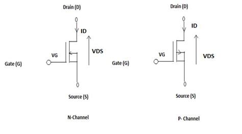
N-Channel MOSFET
In an N-channel MOSFET (NMOS), the substrate is P-type, while the source and drain regions are heavily doped with N-type impurities. When a positive voltage is applied to the gate terminal, it attracts electrons from the P-type substrate to the region beneath the gate oxide, forming an N-type channel between the source and drain. As the gate voltage increases, more electrons accumulate in the channel, increasing its conductivity and allowing current to flow between the source and drain.
P-Channel MOSFET
In a P-channel MOSFET (PMOS), the substrate is N-type, while the source and drain regions are heavily doped with P-type impurities. When a negative voltage is applied to the gate terminal, it repels electrons from the region beneath the gate oxide, creating a P-type channel between the source and drain. As the gate voltage becomes more negative, more holes accumulate in the channel, increasing its conductivity and allowing current to flow between the source and drain.

MOSFET Operation Modes
MOSFETs can operate in three different modes depending on the voltages applied to their terminals:
-
Cut-off Mode: When the gate-source voltage (VGS) is below the threshold voltage (VTH), the MOSFET is in cut-off mode. In this mode, there is no conductive channel between the source and drain, and the device acts as an open switch.
-
Linear Mode (Triode Mode): When VGS > VTH and the drain-source voltage (VDS) is small, the MOSFET operates in linear mode. In this mode, the device acts as a voltage-controlled resistor, and the drain current (ID) is proportional to VDS.
-
Saturation Mode (Active Mode): When VGS > VTH and VDS > VGS – VTH, the MOSFET operates in saturation mode. In this mode, the drain current remains constant and is controlled by the gate-source voltage, making the device suitable for use as an amplifier or current source.

Types of MOSFETs
There are several types of MOSFETs, each with unique characteristics and applications:
-
Enhancement-Mode MOSFET: In this type of MOSFET, there is no conductive channel between the source and drain when the gate-source voltage is zero. A channel is formed when VGS exceeds the threshold voltage. Enhancement-mode MOSFETs are the most common type and are used in various analog and digital circuits.
-
Depletion-Mode MOSFET: In depletion-mode MOSFETs, a conductive channel exists between the source and drain even when the gate-source voltage is zero. Applying a negative VGS for N-channel or a positive VGS for P-channel reduces the channel conductivity. Depletion-mode MOSFETs are less common and are used in specific applications, such as RF switches and high-speed logic circuits.
-
Power MOSFET: Power MOSFETs are designed to handle high currents and voltages. They have a vertical structure with a larger die area to minimize on-resistance and increase current-handling capability. Power MOSFETs are commonly used in switch-mode power supplies, motor drives, and other power electronics applications.
-
LDMOS (Laterally Diffused MOSFET): LDMOS transistors are a type of power MOSFET with a lateral structure, where the current flows parallel to the wafer surface. They offer high breakdown voltage and are commonly used in RF power amplifiers for wireless communication systems.
-
FinFET (Fin Field-Effect Transistor): FinFETs are a type of multi-gate MOSFET where the channel is formed in a thin silicon “fin” that protrudes from the substrate. The gate wraps around the fin, providing better control over the channel and reducing leakage current. FinFETs are widely used in modern high-density integrated circuits, such as microprocessors and memory devices.

MOSFET Parameters
Several key parameters characterize the performance of a MOSFET:
-
Threshold Voltage (VTH): The minimum gate-source voltage required to create a conductive channel between the source and drain. It determines the point at which the MOSFET starts to conduct.
-
On-Resistance (RDS(on)): The resistance between the drain and source terminals when the MOSFET is fully on. A lower RDS(on) is desirable for minimizing power loss and maximizing current-handling capability.
-
Transconductance (gm): The ratio of the change in drain current to the change in gate-source voltage. It represents the amplification factor of the MOSFET and is important for analog applications.
-
Breakdown Voltage (BVDSS): The maximum drain-source voltage that the MOSFET can withstand before breakdown occurs. It determines the voltage-handling capability of the device.
-
Capacitances (CGS, CGD, CDS): The Parasitic Capacitances between the gate-source, gate-drain, and drain-source terminals. These capacitances affect the high-frequency performance and switching speed of the MOSFET.
MOSFET Applications
MOSFETs find applications in a wide range of electronic circuits and systems:
-
Analog Circuits: MOSFETs are used in analog circuits such as amplifiers, filters, and Voltage Regulators. Their voltage-controlled resistance and high Input Impedance make them suitable for these applications.
-
Digital Circuits: MOSFETs are the building blocks of modern digital circuits, including logic gates, memory cells, and microprocessors. Their ability to switch quickly between on and off states enables the implementation of complex digital functions.
-
Power Electronics: Power MOSFETs are extensively used in switch-mode power supplies, DC-DC converters, motor drives, and other power conversion systems. They offer high efficiency, fast switching, and robust performance.
-
RF and Wireless Communication: MOSFETs, particularly LDMOS transistors, are used in RF power amplifiers for wireless communication systems, such as cellular networks and satellite communications. They provide high gain, linearity, and efficiency at RF frequencies.
-
Automotive Electronics: MOSFETs are used in various automotive electronic systems, including engine control units, power steering, and lighting control. They offer reliable performance under harsh environmental conditions and high-temperature operation.
-
Internet of Things (IoT) and Wearable Devices: Low-power MOSFETs are essential components in IoT and wearable devices, where energy efficiency and small form factors are critical. They are used in sensor interfaces, wireless transceivers, and power management circuits.
MOSFET Selection Considerations
When choosing a MOSFET for a specific application, several factors should be considered:
-
Voltage Rating: The MOSFET should have a breakdown voltage (BVDSS) higher than the maximum expected voltage in the circuit to ensure reliable operation and prevent device failure.
-
Current Rating: The continuous drain current rating (ID) should be sufficient to handle the expected load current in the application. The peak current rating should also be considered for pulsed or transient loads.
-
On-Resistance: A lower RDS(on) is desirable to minimize power loss and improve efficiency, especially in power applications. However, MOSFETs with lower RDS(on) typically have higher parasitic capacitances, which can affect switching performance.
-
Switching Speed: The MOSFET’s switching speed, determined by its rise and fall times, should be fast enough to meet the application’s requirements. Faster switching speeds are important for high-frequency and power conversion applications.
-
Package and Thermal Characteristics: The MOSFET package should be suitable for the application’s physical constraints and provide adequate heat dissipation. Proper thermal management is essential to prevent overheating and ensure reliable operation.
-
Cost: The cost of the MOSFET should be considered in the context of the overall system budget and the required performance level. In some cases, a higher-cost MOSFET with better specifications may result in overall system cost savings due to improved efficiency or reliability.
Frequently Asked Questions (FAQ)
- What is the difference between an N-channel and P-channel MOSFET?
-
N-channel MOSFETs have electrons as the majority carriers, while P-channel MOSFETs have holes as the majority carriers. N-channel MOSFETs require a positive gate-source voltage to turn on, while P-channel MOSFETs require a negative gate-source voltage to turn on.
-
Can a MOSFET be used as a switch?
-
Yes, MOSFETs are commonly used as switches in various applications. When operated in the cut-off and saturation modes, MOSFETs can effectively function as voltage-controlled switches, with low on-resistance and high off-resistance.
-
What is the purpose of the gate oxide in a MOSFET?
-
The gate oxide is a thin insulating layer between the gate electrode and the semiconductor substrate. It electrically isolates the gate from the channel, allowing the gate voltage to control the channel conductivity through the field effect. The quality and thickness of the gate oxide are critical for the MOSFET’s performance and reliability.
-
How do power MOSFETs differ from regular MOSFETs?
-
Power MOSFETs are designed to handle high currents and voltages compared to regular MOSFETs. They have a larger die area, vertical structure, and optimized features to minimize on-resistance and increase current-handling capability. Power MOSFETs are commonly used in power electronics applications, such as switch-mode power supplies and motor drives.
-
What is the role of transconductance (gm) in MOSFET amplifiers?
- Transconductance (gm) represents the amplification factor of a MOSFET, relating the change in drain current to the change in gate-source voltage. A higher gm indicates a greater ability to convert input voltage variations into output current variations. In MOSFET amplifiers, a high gm is desirable for achieving high gain and sensitivity.
Conclusion
MOSFETs are versatile and widely used semiconductor devices that have revolutionized the electronics industry. Their voltage-controlled operation, high input impedance, and scalability have made them indispensable in a wide range of applications, from analog and digital circuits to power electronics and wireless communication systems.
Understanding the basic structure, working principle, and types of MOSFETs is crucial for designing and analyzing electronic circuits. By carefully considering factors such as voltage and current ratings, on-resistance, switching speed, and thermal characteristics, engineers can select the most suitable MOSFET for their specific application needs.
As technology advances, MOSFETs continue to evolve, with innovations such as FinFETs and new materials pushing the boundaries of performance, power efficiency, and integration density. These advancements will undoubtedly lead to even more exciting applications and Breakthroughs in the future of electronics.
No responses yet