Introduction to HDI PCB Stackup
High Density Interconnect (HDI) PCBs have become increasingly popular in recent years due to the growing demand for smaller, more complex electronic devices. HDI PCB stackups allow for higher component density and improved signal integrity compared to traditional PCB stackups. However, choosing the right HDI PCB stackup for your specific application can be a challenging task. In this article, we will explore the different types of HDI PCB stackups and help you determine which one is best suited for your PCB design.
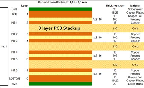
What is an HDI PCB Stackup?
An HDI PCB stackup refers to the arrangement of copper layers, dielectric materials, and interconnections within a printed circuit board. The stackup design plays a crucial role in determining the electrical performance, mechanical stability, and manufacturing feasibility of the PCB. HDI PCB stackups typically involve the use of microvias, buried vias, and blind vias to achieve higher interconnect density and reduce signal path lengths.

Types of HDI PCB Stackups
There are several types of HDI PCB stackups, each with its own advantages and limitations. The most common types include:
1. 1+N+1 Stackup
The 1+N+1 stackup consists of a core layer (N) sandwiched between two outer layers (1+1). The outer layers contain microvias that connect to the adjacent inner layer, while the core layer may contain through-hole vias. This stackup is suitable for designs with moderate complexity and is relatively cost-effective.
| Layer | Description |
|---|---|
| 1 | Outer layer with microvias |
| N | Core layer with through-hole vias |
| 1 | Outer layer with microvias |
2. 2+N+2 Stackup
The 2+N+2 stackup is similar to the 1+N+1 stackup but features two additional outer layers. This allows for more routing flexibility and higher component density. The outer layers contain microvias, while the inner layers may have buried vias or through-hole vias.
| Layer | Description |
|---|---|
| 2 | Outer layers with microvias |
| N | Core layers with buried or through-hole vias |
| 2 | Outer layers with microvias |
3. 3+N+3 Stackup
The 3+N+3 stackup takes the concept further by adding a third set of outer layers. This stackup offers even more routing options and can accommodate highly complex designs. The outer layers contain microvias, and the inner layers may have a combination of buried vias and through-hole vias.
| Layer | Description |
|---|---|
| 3 | Outer layers with microvias |
| N | Core layers with buried or through-hole vias |
| 3 | Outer layers with microvias |
4. Any Layer Via Stackup
An Any Layer Via (ALV) stackup allows for vias to be placed on any layer of the PCB, providing maximum flexibility in routing and component placement. ALV stackups typically use a combination of microvias, buried vias, and through-hole vias to achieve the desired interconnections.
| Layer | Description |
|---|---|
| Any | Microvias, buried vias, or through-hole vias |

Factors to Consider When Choosing an HDI PCB Stackup
When selecting an HDI PCB stackup for your design, there are several factors to consider:
-
Design Complexity: The complexity of your design will dictate the number of layers and types of vias required. More complex designs may require higher layer counts and the use of microvias and buried vias.
-
Signal Integrity: The stackup design should be optimized for signal integrity, minimizing crosstalk, impedance mismatch, and signal reflections. Proper grounding and shielding techniques should be employed to ensure reliable performance.
-
Manufacturing Capability: The chosen stackup must be compatible with the manufacturing capabilities of your PCB fabricator. Some stackups may require advanced manufacturing processes or materials that not all fabricators can accommodate.
-
Cost: Higher layer counts and more complex stackups generally increase the manufacturing cost of the PCB. It is essential to strike a balance between performance requirements and cost considerations.
-
Thermal Management: The stackup design should take into account the thermal management needs of the PCB. Proper heat dissipation is crucial for maintaining the reliability and longevity of the electronic components.

HDI PCB Stackup Design Guidelines
To ensure the success of your HDI PCB design, follow these general guidelines:
-
Minimize Layer Count: Use the minimum number of layers necessary to meet your design requirements. Excessive layering can increase manufacturing complexity and cost.
-
Optimize Via Placement: Place vias strategically to minimize signal path lengths and reduce the number of layer transitions. Avoid placing vias in critical signal paths or under components whenever possible.
-
Maintain Symmetry: Strive for a symmetrical stackup design to minimize warpage and ensure even distribution of stresses during manufacturing.
-
Consider Impedance Control: Use controlled impedance techniques, such as differential pairs and impedance-matched traces, to maintain signal integrity and minimize reflections.
-
Adhere to Manufacturing Constraints: Consult with your PCB fabricator to understand their manufacturing capabilities and design rules. Adhere to the recommended minimum feature sizes, spacing, and drill sizes to ensure manufacturability.
Frequently Asked Questions (FAQ)
-
Q: What is the difference between microvias, buried vias, and blind vias?
A: Microvias are small-diameter vias that connect adjacent layers, typically with a diameter less than 6 mils. Buried vias are used to connect internal layers without penetrating the outer layers, while blind vias connect an outer layer to an internal layer without going through the entire board thickness. -
Q: How do I choose the right dielectric material for my HDI PCB stackup?
A: The choice of dielectric material depends on factors such as the desired electrical performance, thermal requirements, and manufacturing process. Common dielectric materials for HDI PCBs include FR-4, polyimide, and high-frequency laminates like Rogers or Isola materials. Consult with your PCB fabricator for recommendations based on your specific design requirements. -
Q: Can I mix different via types in the same HDI PCB stackup?
A: Yes, it is possible to use a combination of microvias, buried vias, and through-hole vias in the same stackup. This approach allows for greater flexibility in routing and component placement, but it may increase manufacturing complexity and cost. -
Q: How does the aspect ratio of vias affect the manufacturability of HDI PCBs?
A: The aspect ratio of a via refers to the ratio of its depth to its diameter. High aspect ratio vias (greater than 8:1) can be challenging to manufacture reliably, especially for small-diameter microvias. It is essential to consider the aspect ratio when designing your HDI PCB stackup and to consult with your PCB fabricator for their recommended guidelines. -
Q: What are the advantages of using an Any Layer Via (ALV) stackup?
A: An ALV stackup offers the highest level of flexibility in routing and component placement by allowing vias to be placed on any layer of the PCB. This can help reduce layer count, improve signal integrity, and optimize board space utilization. However, ALV stackups may require advanced manufacturing capabilities and increase fabrication costs compared to simpler stackups.
Conclusion
Choosing the right HDI PCB stackup is crucial for achieving the desired electrical performance, mechanical stability, and manufacturability of your PCB design. By understanding the different types of HDI PCB stackups and considering factors such as design complexity, signal integrity, manufacturing capability, cost, and thermal management, you can make an informed decision that meets your specific requirements.
When designing your HDI PCB stackup, follow best practices such as minimizing layer count, optimizing via placement, maintaining symmetry, considering impedance control, and adhering to manufacturing constraints. Collaborating closely with your PCB fabricator throughout the design process can help ensure the success of your HDI PCB project.
By selecting the appropriate HDI PCB stackup and following sound design principles, you can unlock the full potential of high-density interconnect technology and create innovative, reliable, and cost-effective electronic products.
No responses yet