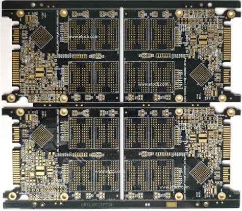
What is an HDI PCB?
An HDI PCB is a printed circuit board that features higher wiring density per unit area than traditional PCBs. This is achieved through the use of smaller vias, finer trace widths, and smaller component pitch. HDI PCBs can have multiple layers, with the most common configurations being 4, 6, 8, and 10 layers. The increased density allows for more compact designs, making HDI PCBs ideal for applications where space is limited, such as smartphones, wearables, and medical devices.
Advantages of HDI PCBs
Reduced Size and Weight
One of the primary advantages of HDI PCBs is their ability to reduce the overall size and weight of electronic devices. By utilizing smaller vias, finer trace widths, and smaller component pitch, designers can create more compact PCB layouts. This reduction in size and weight is particularly beneficial for portable devices, where every millimeter and gram counts.
Improved Signal Integrity
HDI PCBs offer improved signal integrity compared to traditional PCBs. The shorter trace lengths and reduced layer count minimize signal distortion and crosstalk, resulting in cleaner and more reliable signal transmission. This is especially important for high-speed applications, such as 5G communication systems and high-performance computing.
Enhanced Functionality
The increased wiring density of HDI PCBs allows for the integration of more components and features within a smaller footprint. This enhanced functionality enables designers to create more sophisticated and feature-rich devices without compromising on size. HDI PCBs are particularly well-suited for applications that require a high level of integration, such as system-on-chip (SoC) designs and multi-chip modules (MCMs).
HDI PCB Design Considerations
Layer Stack-up
The layer stack-up is a crucial aspect of HDI PCB design, as it determines the number and arrangement of layers within the PCB. When designing an HDI PCB, it is essential to consider the following factors:
- Number of layers: HDI PCBs typically have 4, 6, 8, or 10 layers. The number of layers required depends on the complexity of the design and the desired functionality.
- Layer arrangement: The arrangement of layers should be optimized for signal integrity and manufacturability. Common layer arrangements for HDI PCBs include 1+N+1 (where N represents the number of inner layers) and 2+N+2.
- Dielectric material: The choice of dielectric material affects the PCB’s electrical properties, such as impedance and signal speed. Common dielectric materials for HDI PCBs include FR-4, Rogers, and Isola.
Via Types and Sizes
HDI PCBs utilize various types of vias to achieve higher wiring density and improved signal integrity. The most common via types used in HDI PCB design are:
| Via Type | Description | Typical Size Range |
|---|---|---|
| Through Hole | Drilled through the entire PCB thickness | 0.2mm – 0.4mm |
| Blind | Drilled from the surface to an inner layer | 0.1mm – 0.2mm |
| Buried | Drilled between inner layers, not visible from the surface | 0.1mm – 0.15mm |
| Micro | Laser-drilled, used for high-density interconnects | 0.05mm – 0.1mm |
When selecting via types and sizes for your HDI PCB design, consider the following factors:
- Space constraints: Smaller vias allow for higher wiring density but may be more challenging to manufacture.
- Signal integrity: Blind and buried vias can improve signal integrity by reducing the via stub effect.
- Cost: Smaller vias and advanced via types may increase manufacturing costs.
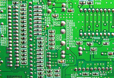
Trace Width and Spacing
Trace width and spacing are critical parameters in HDI PCB design, as they directly impact wiring density and signal integrity. When designing traces for an HDI PCB, consider the following guidelines:
- Use the narrowest trace width that can be reliably manufactured and meets the current carrying capacity requirements.
- Maintain adequate spacing between traces to minimize crosstalk and signal distortion.
- Follow the manufacturer’s design rules and guidelines for minimum trace width and spacing.
Typical trace width and spacing for HDI PCBs range from 0.075mm to 0.15mm, depending on the PCB manufacturer’s capabilities and the specific design requirements.
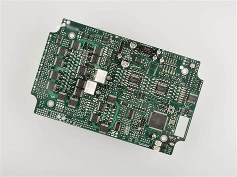
Component Selection and Placement
Component selection and placement play a crucial role in HDI PCB design, as they affect the overall size, performance, and manufacturability of the PCB. When selecting and placing components on an HDI PCB, consider the following factors:
- Package size: Use the smallest component packages that meet the design requirements to minimize the PCB footprint.
- Pitch: Select components with a fine pitch to enable higher wiring density.
- Placement: Optimize component placement for signal integrity, thermal management, and manufacturability.
- Routing: Consider the routing implications of component placement, such as the number of layers required and the use of blind and buried vias.

HDI PCB Design Tools
To create a successful HDI PCB design, it is essential to use the right design tools. Some popular HDI PCB design tools include:
- Altium Designer
- Cadence Allegro
- Mentor Graphics PADS
- Zuken CR-8000
These tools offer advanced features specifically tailored for HDI PCB design, such as:
- Automated via placement and optimization
- High-speed design analysis and simulation
- Design rule checking (DRC) for HDI-specific constraints
- 3D modeling and visualization
When selecting an HDI PCB design tool, consider factors such as ease of use, compatibility with your existing design workflow, and the availability of HDI-specific features and libraries.
HDI PCB Manufacturing Process
The manufacturing process for HDI PCBs is more complex than that of traditional PCBs due to the smaller features and advanced via technologies involved. The typical HDI PCB manufacturing process includes the following steps:
- Material selection: Choose the appropriate base material, such as FR-4 or Rogers, based on the design requirements.
- Lamination: Laminate the core layers together to form the PCB stack-up.
- Drilling: Drill through holes, blind vias, and buried vias using mechanical or laser drilling techniques.
- Plating: Plate the drilled holes and vias with copper to create electrical connections between layers.
- Patterning: Create the trace patterns on the outer and inner layers using photolithography and etching processes.
- Solder mask application: Apply a solder mask to protect the traces and prevent short circuits.
- Surface finish: Apply a surface finish, such as ENIG or HASL, to protect the exposed copper and facilitate soldering.
- Electrical testing: Perform electrical tests to ensure the PCB functions as intended and meets the design specifications.
When working with an HDI PCB manufacturer, it is essential to communicate your design requirements clearly and ensure that the manufacturer has the necessary capabilities and experience to produce your HDI PCB reliably.
HDI PCB Design Best Practices
To ensure a successful HDI PCB design, follow these best practices:
- Start with a clear understanding of your design requirements, including functionality, size constraints, and performance targets.
- Choose the appropriate layer stack-up and via types based on your design requirements and the manufacturer’s capabilities.
- Use the smallest trace widths and spacings that can be reliably manufactured and meet the design requirements.
- Optimize component selection and placement for signal integrity, thermal management, and manufacturability.
- Use appropriate design tools and follow the manufacturer’s design rules and guidelines.
- Collaborate closely with your HDI PCB manufacturer throughout the design and manufacturing process to ensure a successful outcome.
Frequently Asked Questions (FAQ)
- What is the difference between an HDI PCB and a traditional PCB?
-
An HDI PCB features higher wiring density per unit area than a traditional PCB, achieved through the use of smaller vias, finer trace widths, and smaller component pitch. This allows for more compact designs and improved signal integrity.
-
What are the most common layer configurations for HDI PCBs?
-
The most common layer configurations for HDI PCBs are 4, 6, 8, and 10 layers. The number of layers required depends on the complexity of the design and the desired functionality.
-
What are the advantages of using blind and buried vias in HDI PCB design?
-
Blind and buried vias can improve signal integrity by reducing the via stub effect. They also enable higher wiring density and more compact designs by freeing up space on the outer layers of the PCB.
-
How do I select the appropriate trace width and spacing for my HDI PCB design?
-
Use the narrowest trace width that can be reliably manufactured and meets the current carrying capacity requirements. Maintain adequate spacing between traces to minimize crosstalk and signal distortion. Follow the manufacturer’s design rules and guidelines for minimum trace width and spacing.
-
What should I consider when choosing an HDI PCB manufacturer?
- When choosing an HDI PCB manufacturer, consider factors such as their experience with HDI PCB fabrication, their manufacturing capabilities (e.g., minimum via sizes and trace widths), their quality control processes, and their ability to meet your project’s timeline and budget requirements. It is also essential to establish clear communication and collaborate closely with your manufacturer throughout the design and manufacturing process.
In conclusion, HDI PCB design offers numerous advantages for creating compact, high-performance electronic devices. By understanding the key design considerations, such as layer stack-up, via types, trace widths, and component selection, and following best practices, you can create the most suitable HDI PCB for your specific needs. Collaborating closely with an experienced HDI PCB manufacturer and using the right design tools will ensure a successful outcome for your HDI PCB project.
No responses yet