Introduction to Embedded PCB Technology
Embedded PCB, also known as embedded printed circuit board, is a cutting-edge technology in the electronics industry that integrates electronic components within the layers of a multi-layer circuit board. This innovative approach to PCB design and manufacturing offers numerous advantages over traditional surface-mount technology (SMT) and through-hole mounting techniques.
In an embedded PCB, passive components such as resistors, capacitors, and inductors are embedded into the inner layers of the circuit board, while active components like integrated circuits (ICs) and connectors are mounted on the surface. This unique combination of embedded and surface-mounted components enables the creation of highly compact, reliable, and high-performance electronic devices.
Benefits of Embedded PCB Technology
-
Space Savings: By embedding components within the layers of the PCB, the overall footprint of the circuit board can be significantly reduced, allowing for more compact and lightweight electronic devices.
-
Improved Electrical Performance: Embedding components closer to the interconnects reduces the distance that signals must travel, resulting in improved signal integrity, reduced noise, and enhanced electromagnetic compatibility (EMC).
-
Increased Reliability: Embedded components are protected from external factors such as mechanical stress, moisture, and temperature fluctuations, leading to higher reliability and longer product life.
-
Cost Reduction: Although the initial investment in embedded PCB technology may be higher, the overall cost of the final product can be reduced due to the smaller form factor, fewer assembly steps, and improved yield.
Design Considerations for Embedded PCB
Component Selection
When designing an embedded PCB, careful consideration must be given to the selection of components that will be embedded within the layers of the board. The following factors should be taken into account:
-
Size: Embedded components must be small enough to fit within the thickness of the PCB layers without compromising the structural integrity of the board.
-
Termination Type: Components with suitable termination types, such as leadless chip resistors (LCRs) and leadless chip capacitors (LCCs), are preferred for embedding.
-
Power Rating: The power rating of the embedded components should be chosen based on the specific application requirements and the thermal dissipation capabilities of the PCB.
Layer Stack-up Design
The layer stack-up of an embedded PCB plays a crucial role in determining the electrical performance and manufacturability of the board. A typical embedded PCB stack-up may consist of the following layers:
| Layer | Description |
|---|---|
| Top Layer | Surface-mounted components and interconnects |
| Embedded Layer 1 | Embedded passive components and interconnects |
| Ground Plane | Provides a low-impedance return path for signals |
| Embedded Layer 2 | Embedded passive components and interconnects |
| Power Plane | Distributes power to the components |
| Bottom Layer | Surface-mounted components and interconnects |
The number and arrangement of layers may vary depending on the complexity of the design and the specific requirements of the application.
Design for Manufacturability (DFM)
To ensure the successful fabrication and assembly of an embedded PCB, several design for manufacturability (DFM) guidelines must be followed:
-
Clearance and Spacing: Adequate clearance and spacing must be maintained between embedded components, interconnects, and other features to prevent short circuits and ensure reliable operation.
-
Via Placement: Vias should be strategically placed to provide electrical connections between layers while avoiding interference with embedded components.
-
Thermal Management: Proper thermal management techniques, such as the use of thermal vias and heat spreaders, should be employed to dissipate heat generated by the embedded components.
Manufacturing Process for Embedded PCB
The manufacturing process for an embedded PCB involves several specialized steps that differ from traditional PCB fabrication methods.
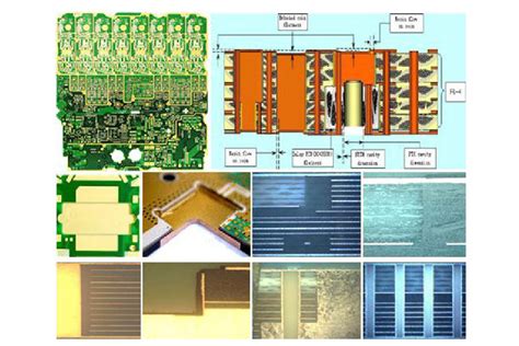
Cavity Formation
The first step in the embedded PCB manufacturing process is the formation of cavities within the PCB layers to accommodate the embedded components. There are two primary methods for creating cavities:
-
Mechanical Drilling: High-precision drilling machines are used to create cavities of specific sizes and shapes in the PCB layers.
-
Laser Ablation: Advanced laser systems are employed to selectively remove material from the PCB layers, creating cavities with high accuracy and minimal damage to the surrounding areas.
Component Placement
Once the cavities have been formed, the embedded components are placed into the designated locations within the PCB layers. This process is typically performed using automated pick-and-place machines that are programmed to handle the specific components and their orientations.
Lamination and Pressing
After the components have been placed, the PCB layers are stacked together and laminated under high pressure and temperature. This process bonds the layers together and encapsulates the embedded components within the board.
Drilling and Plating
Following lamination, the embedded PCB undergoes drilling and plating processes to create the necessary electrical connections between layers. This includes the formation of vias, which are small holes that are drilled through the layers and plated with a conductive material to establish electrical paths.
Surface Mounting and Finishing
The final steps in the embedded PCB manufacturing process involve the surface mounting of additional components, such as ICs and connectors, and the application of protective finishes, such as solder mask and surface finish coatings.

Applications of Embedded PCB Technology
Embedded PCB technology finds applications in a wide range of industries where high-density, high-performance, and reliability are crucial. Some notable applications include:
-
Aerospace and Defense: Embedded PCBs are used in avionics, satellite systems, and military equipment where space constraints and harsh environmental conditions demand robust and reliable electronics.
-
Medical Devices: Implantable medical devices, such as pacemakers and neurostimulators, benefit from the miniaturization and reliability offered by embedded PCB technology.
-
Automotive Electronics: Advanced driver assistance systems (ADAS), infotainment systems, and powertrain control modules increasingly rely on embedded PCBs for enhanced functionality and performance.
-
Consumer Electronics: Smartphones, wearables, and IoT devices leverage embedded PCB technology to achieve compact form factors and improved power efficiency.
Future Trends and Challenges
As the demand for smaller, faster, and more reliable electronic devices continues to grow, embedded PCB technology is expected to evolve and address new challenges.
Advanced Materials
The development of advanced materials, such as high-density interconnect (HDI) substrates and low-loss dielectrics, will enable the creation of even more compact and high-performance embedded PCBs.
3D Integration
The integration of embedded components in three-dimensional (3D) PCB structures, such as package-on-package (PoP) and system-in-package (SiP) configurations, will further push the boundaries of miniaturization and functionality.
Challenges
Despite the numerous benefits of embedded PCB technology, there are several challenges that must be addressed:
-
Design Complexity: The design of embedded PCBs requires specialized knowledge and tools to ensure optimal component placement, signal integrity, and thermal management.
-
Manufacturing Challenges: The fabrication and assembly of embedded PCBs involve complex processes that require precise control and specialized equipment, leading to higher initial costs and longer lead times.
-
Testing and Inspection: The embedded nature of the components makes testing and inspection more challenging, requiring advanced techniques such as 3D X-ray imaging and automated optical inspection (AOI) to ensure quality and reliability.
Frequently Asked Questions (FAQ)
- What is the difference between an embedded PCB and a traditional PCB?
-
In an embedded PCB, passive components are embedded within the layers of the board, while in a traditional PCB, all components are mounted on the surface.
-
Can any component be embedded in a PCB?
-
Not all components are suitable for embedding. Passive components with small footprints and appropriate termination types, such as chip resistors and capacitors, are most commonly embedded.
-
How does embedding components affect the electrical performance of a PCB?
-
Embedding components reduces the distance that signals must travel, resulting in improved signal integrity, reduced noise, and enhanced electromagnetic compatibility (EMC).
-
Are embedded PCBs more expensive than traditional PCBs?
-
The initial investment in embedded PCB technology may be higher due to the specialized design, manufacturing, and testing processes involved. However, the overall cost of the final product can be reduced due to the smaller form factor, fewer assembly steps, and improved yield.
-
What industries are most likely to benefit from embedded PCB technology?
- Industries that require high-density, high-performance, and reliable electronics, such as aerospace, defense, medical devices, automotive, and consumer electronics, are most likely to benefit from embedded PCB technology.
Conclusion
Embedded PCB technology represents a significant advancement in the field of electronics packaging, offering numerous benefits such as space savings, improved electrical performance, increased reliability, and potential cost reduction. By integrating passive components within the layers of a multi-layer circuit board and combining them with surface-mounted active components, embedded PCBs enable the creation of highly compact, efficient, and robust electronic devices.
However, the adoption of embedded PCB technology also presents challenges in terms of design complexity, manufacturing processes, and testing and inspection. As the electronics industry continues to evolve and demand more advanced packaging solutions, embedded PCB technology is expected to play an increasingly important role in shaping the future of electronic devices.
No responses yet